’C209 Memory and I/O Spaces
11-9
TMS320C209
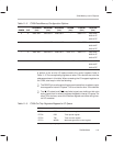
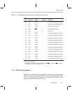
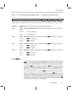
Table 11–2. ’C209 Data-Memory Configuration Options
RAMEN CNF
DARAM B0
(hex)
DARAM B1
(hex)
DARAM B2
(hex)
SARAM
(hex)
External
(hex)
Reserved
(hex)
0 0 0200–02FF 0300–03FF 0060–007F – 0800–FFFF 0000–005F
0080–01FF
0400–07FF
0 1 – 0300–03FF 0060–007F – 0800–FFFF 0000–005F
0080–02FF
0400–07FF
1 0 0200–02FF 0300–03FF 0060–007F 1000–1FFF 2000–FFFF 0000–005F
0080–01FF
0400–0FFF
1 1 – 0300–03FF 0060–007F 1000–1FFF 2000–FFFF 0000–005F
0080–02FF
0400–0FFF
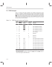
A portion of the on-chip I/O space contains the control registers listed in
Table 11–3.The corresponding registers on other ’C2xx devices are not at the
addresses shown in this table. When accessing the I/O-mapped registers on
the ’C209, also keep in mind the following:
The READY pin must be pulled high to permit reads from or writes to regis-
ters mapped to internal I/O space. This is not true for other ’C2xx devices.
The IS (I/O select) and R/W (read/write) signals are visible on their pins
during reads from or writes to registers mapped to internal I/O space. On
other ’C2xx devices, none of the interface signals are visible during inter-
nal I/O accesses.
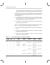
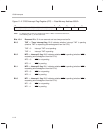
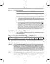
Table 11–3. ’C209 On-Chip Registers Mapped to I/O Space
I/O Address Name Description
FFFCh TCR Timer control register
FFFDh PRD Timer period register
FFFEh TIM Timer counter register
FFFFh WSGR Wait-state generator control register
Note: The corresponding registers on other ’C2xx devices are not at these addresses.


