


Emulation Design Considerations
E-21
Design Considerations for Using XDS510 Emulator
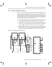
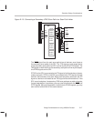
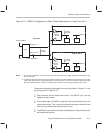
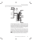
Figure E–11. EMU0/1 Configuration to Meet Timing Requirements of Less Than 25 ns
Open-
collector
drivers
EMU0/1-IN
Backplane
Target board m
TCK
XCNT_ENABLE
To emulator EMU0
PAL
Pullup
resistor
Open-
collector
drivers
Target board 1
EMU0/1
EMU0/1-OUT
. . .
Device
Device
EMU0/1
. . .
. . .
. . .
. . .
. . .
1n
Device
Device
1n
Pullup
resistor
Pullup
resistor
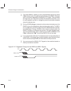
Notes: 1) The low time on EMU0/1-IN should be at least one TCK cycle and less than 10 s. Software sets the EMU0/1-OUT
pin to a high state.
2) To enable the open-collector driver and pullup resistor on EMU1 to provide rise/fall times of less than 25 ns, the modifi-
cation shown in this figure is suggested. Rise times of more than 25 ns can cause the emulator to detect false edges
during the RUNB command or when the external counter selected from the debugger analysis menu is used.
These seven important points apply to the circuitry shown in Figure E–11 and
the timing shown in Figure E–12:
Open-collector drivers isolate each board. The EMU0/1 pins are tied
together on each board.
At the board edge, the EMU0/1 signals are split to provide both input and
output connections. This is required to prevent the open-collector drivers
from acting as latches that can be set only once.
The EMU0/1 signals are bused down the backplane. Pullup resistors must
be installed as required.