Emulation Design Considerations
E-17
Design Considerations for Using XDS510 Emulator
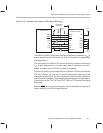
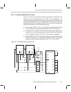
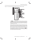
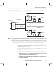
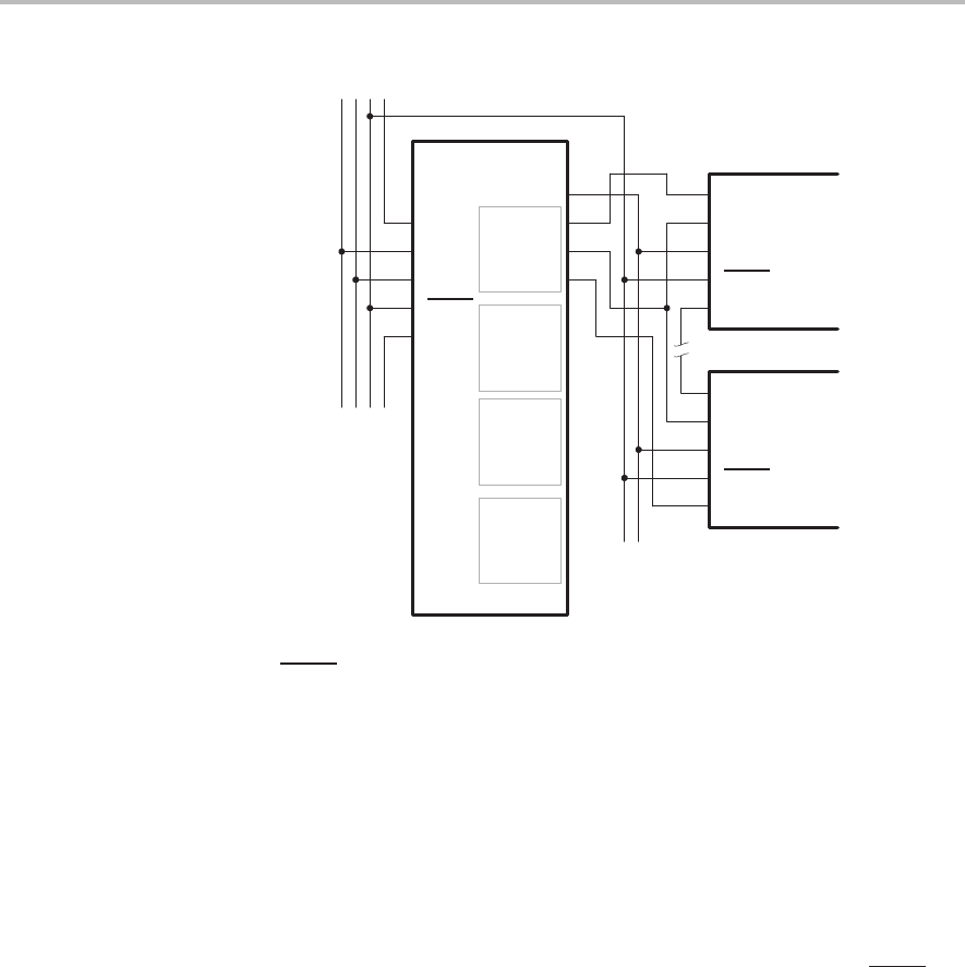
Figure E–10. Connecting a Secondary JTAG Scan Path to a Scan Path Linker
TDI
TCK
TDO
TRST
TMS
TDO
TRST
TCK
TMS
TDI
DTDI0
DTMS0
DTDO0
DTCK
TDO
TRST
TCK
TMS
TDI
SPL
JTAG 0
JTAG N
DTDI1
DTMS1
DTDO1
DTDI2
DTMS2
DTDO2
DTDI3
DTMS3
DTDO3
. . .
The TRST signal from the main scan path drives all devices, even those on
the secondary scan paths of the SPL. The TCK signal on each target device
on the secondary scan path of an SPL is driven by the SPL’s DTCK signal. The
TMS signal on each device on the secondary scan path is driven by the respec-
tive DTMS signals on the SPL.
DTDO0 on the SPL is connected to the TDI signal of the first device on the sec-
ondary scan path. DTDI0 on the SPL is connected to the TDO signal of the last
device in the secondary scan path. Within each secondary scan path, the TDI
signal of a device is connected to the TDO signal of the device before it. If the
SPL is on a backplane, its secondary JTAG scan paths are on add-on boards;
if signal degradation is a problem, you may need to buffer both the TRST
and
DTCK signals. Although degradation is less likely for DTMS
n
signals, you may
also need to buffer them for the same reasons.


