


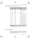
’C209 Memory and I/O Spaces
11-7
TMS320C209
Do Not Write to Reserved Addresses
To avoid unpredictable operation of the processor, do not write to
any addresses labeled Reserved. This includes any data-memory
address in the range 0000h–005Fh that is not designated for an
on-chip register and any I/O address in the range FF00h–FFFFh
that is not designated for an on-chip register.
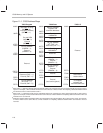
You select or deselect the ROM by changing the level on the MP/MC
pin at re-
set:
When MP/MC = 0 (low) at reset, the device is configured as a microcom-
puter. The on-chip ROM is enabled and is accessible at addresses
0000h–0FFFh. The device fetches the reset vector from on-chip ROM.
When MP/MC = 1 (high) at reset, the device is configured as a micropro-
cessor, and addresses 0000h–0FFFh are used to access external
memory. The device fetches the reset vector from external memory.
Regardless of the value of MP/MC
, the ’C2xx fetches its reset vector at location
0000h of program memory.
The addresses assigned to the on-chip SARAM are shared by program
memory and data memory. The RAMEN signal allows you to toggle the data
addresses 1000h–1FFFh and the program addresses 1000h–1FFFh between
on-chip memory and external memory:
When RAMEN = 1 (high), program addresses 1000h–1FFFh and data
addresses 1000h–1FFFh are mapped to the same physical locations in
the on-chip SARAM. For example, 1000h in program memory and 1000h
in data memory point to the same physical location in the on-chip SARAM.
Thus, the 4K words of on-chip SARAM are accessible for program and/or
data space.
Note:
When RAMEN = 1, program addresses 1000h–1FFFh and data addresses
1000h–1FFFh are one and the same. When writing data to these locations
be careful not to overwrite existing program instructions.
When RAMEN = 0 (low), program addresses 1000h–1FFFh (4K) are
mapped to external program memory and data addresses 1000h–1FFFh