Instruction Set Comparison Table
B-21
TMS320C1x/C2x/C2xx/C5x Instruction Set Comparison
Syntax
Description5x2xx2x1x
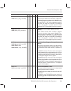
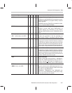
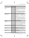
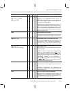
LDP
dma
LDP {
ind
} [
, next ARP
]
LDP #
k
√
√
√
√
√
√
√
√
√
√
Load Data-Memory Page Pointer
TMS320C1x devices: Load the LSB of the contents of
the addressed data-memory location into the DP regis-
ter. All high-order bits are ignored. DP = 0 defines page
0 (words 0–127), and DP = 1 defines page 1 (words
128–143/255).
TMS320C2x, TMS320C2xx, and TMS320C5x de-
vices: Load the 9 LSBs of the addressed data-memory
location or a 9-bit immediate value into the DP register.
The DP and 7-bit data-memory address are concate-
nated to form 16-bit data-memory addresses.
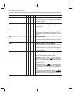
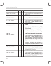
LDPK
1-bit constant
LDPK
9-bit constant
√
√ √ √
Load Data-Memory Page Pointer Immediate
TMS320C1x devices: Load a 1-bit immediate value
into the DP register. DP = 0 defines page 0 (words
0–127), and DP = 1 defines page 1 (words
128–143/255).
TMS320C2x, TMS320C2xx, and TMS320C5x de-
vices: Load a 9-bit immediate into the DP register. The
DP and 7-bit data-memory address are concatenated
to form 16-bit data-memory addresses. DP 8 speci-
fies external data memory. DP = 4 through 7 specifies
on-chip RAM blocks B0 or B1. Block B2 is located in
the upper 32 words of page 0.
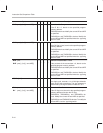
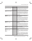
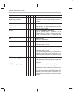
LMMR
dma,
#
lk
LMMR {
ind
}
,
#
lk
[
, next ARP
]
√
√
Load Memory-Mapped Register
Load the contents of the memory-mapped register
pointed at by the 7 LSBs of the direct or indirect data-
memory value into the long immediate addressed
data-memory location. The 9 MSBs of the data-
memory address are cleared, regardless of the current
value of DP or the 9 MSBs of AR (ARP).
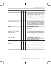
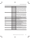
LPH
dma
LPH {
ind
} [
, next ARP
]
√
√
√
√
√
√
Load High P Register
Load the contents of the addressed data-memory lo-
cation into the 16 MSBs of the P register; the LSBs are
not affected.
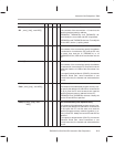
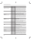
LRLK
AR, lk
√ √ √
Load Auxiliary Register Long Immediate
Load a 16-bit immediate value into the designated aux-
iliary register.
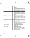
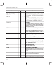
LST
dma
LST {
ind
} [
, next ARP
]
√
√
√
√
√
√
√
√
Load Status Register
Load the contents of the addressed data-memory
location into the ST (TMS320C1x) or into ST0
(TMS320C2x/2xx/5x).


