


I/O Space
4-24
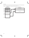
The map has three main sections of addresses:
Addresses 0000h–FEFFh allow access to off-chip peripherals typically
used in DSP applications, such as digital-to-analog and analog-to-digital
converters.
Addresses FF00h–FF0Fh are mapped to on-chip I/O space. These ad-
dresses are reserved for test purposes and should not be used.
Addresses FF10h–FFFFh are also mapped to on-chip I/O space. These
addresses are used for other reserved space and for the on-chip I/O-
mapped registers. For ’C2xx devices other than the ’C209, Table 4–4 lists
the registers mapped to on-chip I/O space. For the I/O-mapped registers
on the ’C209, see Section 11.2, on page 11-5.
Do Not Write to Reserved Addresses
To avoid unpredictable operation of the processor, do not write to
I/O addresses FF00h–FF0Fh or any reserved I/O address in the
range FF10–FFFFh (that is, any address not designated for an
on-chip peripheral.)
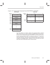
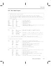
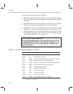
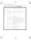
Table 4–4. On-Chip Registers Mapped to I/O Space
I/O Address Name Description
FFE8h CLK CLK register
FFECh ICR Interrupt control register
FFF0h SDTR Synchronous serial port transmit and receive register
FFF1h SSPCR Synchronous serial port control register
FFF4h ADTR Asynchronous serial port transmit and receive register
FFF5h ASPCR Asynchronous serial port control register
FFF6h IOSR Input/output status register
FFF7h BRD Baud rate divisor register
FFF8h TCR Timer control register
FFF9h PRD Timer period register
FFFAh TIM Timer counter register
FFFCh WSGR Wait-state generator control register
Note: This table does not apply to the ’C209. For the I/O-mapped registers on the ’C209,
see Section 11.2 on page 11-5.