


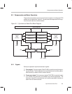
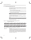
Components and Basic Operation
9-4
Data signal. The data signal carries the actual data that is transferred in
the transmit/receive operation. The data signal transmit pin (DX) of one
device should be connected to the data signal receive (DR) pin on another
device.
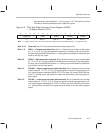
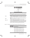
Table 9–1 describes the six pins that use these signals.
Table 9–1. SSP Interface Pins
Pin
Name
Description
CLKX
Transmit clock input or output.
The clock signal is used for clocking data
from the serial port transmit shift register (XSR) to the DX pin. If the port is
configured for accepting an external clock, this pin receives the clock sig-
nal. If the port is configured for generating an internal clock, this pin trans-
mits the clock signal.
FSX
Transmit frame synchronization.
FSX signals the start of a transmission.
If the port is configured for accepting an external frame sync pulse, this pin
receives the pulse. If the port is configured for generating an internal frame
sync pulse, this pin transmits the signal.
DX
Serial data transmit.
DX transmits serial data from the serial port transmit
shift register (XSR).
CLKR
Receive clock input.
CLKR receives an external clock signal for clocking
the data from the DR pin into the serial port receive shift register (RSR).
FSR
Receive frame synchronization.
FSR initiates the reception of data at the
beginning of the packet.
DR
Serial data receive.
DR receives serial data, transferring it into the serial
port receive shift register (RSR).
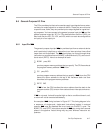
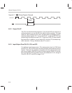
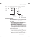
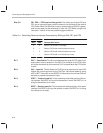
Figure 9–2 shows how the signals are connected in a typical serial transfer be-
tween two devices. The DR pin receives serial data from the D
OUT
signal, and
the DX signal sends serial data to the D
IN
pin. The FSX and FSR signals are
both supplied from the FS
pin, and they initiate the transfers (at the beginning
of a data packet). The SCK signal drives both the CLKX and CLKR signals,
which clock the bit transfers.