


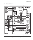
Hardware Description
3-40 Copyright © 2003-2007 ARM Limited. All rights reserved. ARM DUI 0224F
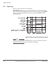
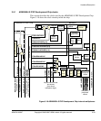
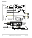
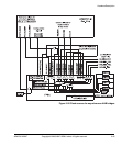
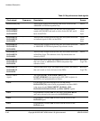
Table 3-5 lists the clock signals.
Table 3-5 ARM926EJ-S PXP Development Chip clocks
Clock signal Frequency Description Source
GLOBALCLK 6–75MHz This is a master clock that is shared between the FPGA, Logic Tile,
and ARM926EJ-S PXP Development Chip.
ICS307
OSC0
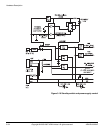
HCLKM1 6–50MHz The AHB master interface clock is used by the AHB Bridge 1 to
off-chip peripherals when it operates in asynchronous mode. By
default, the multiplexor selects GLOBALCLK (driven by OSC0)
as the external clock source.
Note
By default, the AHB M1, AHB M2, and AHB S bridges all operate
in synchronous mode and the external reference clocks are ignored.
ICS307
OSC1
HCLKM2 6–40MHz The AHB master interface clock is used by the AHB Bridge 2 to
off-chip peripherals when it operates in asynchronous mode. By
default, the multiplexor selects GLOBALCLK (driven by OSC0)
as the external clock source.
ICS307
OSC2
HCLKS 6–33MHz The AHB master interface clock is used by the AHB Bridge to
on-chip peripherals when it operates in asynchronous mode. By
default, the multiplexor selects GLOBALCLK (driven by OSC0)
as the external clock source.
ICS307
OSC3
PLLCLKEXT 6–200MHz When the development chip PLL is not used, this input can be used
to drive the CPU and AMBA clocks. This clock is selected by the
Clock and Reset Controller which is controlled by the System
Controller.
Note
By default, the ARM926EJ-S PXP Development Chip uses a PLL
to generate the CPU and AMBA clocks based on the
XTALCLKEXT signal. PLLCLKEXT and REFCLK32K are
not used.
ICS307
OSC0
REFCLK32K 32.768kHz
(fixed)
This clock is selected by the Clock and Reset Controller which is
controlled by the System Controller. This signal is also used to
generate a 1Hz clock for the Real Time Clock. When the
development chip PLL is not used, this input can be used to drive
the CPU and AMBA clocks.
Crystal