


RealView Logic Tile
ARM DUI 0224F Copyright © 2003-2007 ARM Limited. All rights reserved. F-5
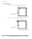
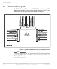
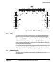
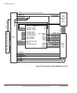
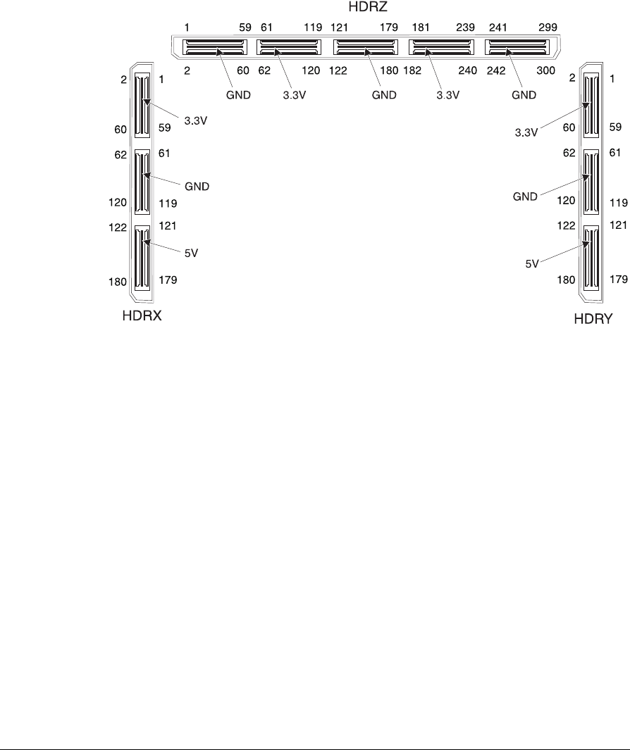
Figure F-3 HDRX, HDRY, and HDRZ (upper) pin numbering
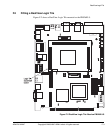
F.3.1 JTAG
The JTAG signals for the FPGA on the RealView Logic Tile are routed through the
headers to the tile at the top of the stack and from there back down through the tile.
There is not a JTAG connector on the RealView Logic Tile. Use the JTAG or USB debug
connector on the PB926EJ-S.
If multiple RealView Logic Tiles are stacked on a PB926EJ-S, the JTAG equipment is
always connected to the PB926EJ-S and the signals are routed upwards to the top tile
and then back down to the PB926EJ-S.
Use the JTAG interface to program the configuration flash in the RealView Logic Tile
or to directly load the RealView Logic Tile FPGA image. For more information on
JTAG signals, see JTAG and USB debug port support on page 3-96.
F.3.2 Variable I/O levels
All HDRX, HDRY, and HDRZ connector signals on the PB926EJ-S are fixed at 3.3V
I/O signalling level.