


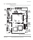
Signal Descriptions
ARM DUI 0224F Copyright © 2003-2007 ARM Limited. All rights reserved. A-35
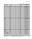
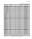
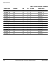
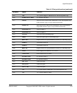
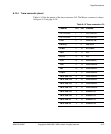
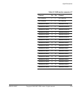
TP15 1V8 1.8 V power supply to ARM926EJ-S PXP Development Chip
TP16 SCIDATAOUTTDD0 SC interface data out 0
TP17 SIRIN0 IrDA in 0 from UART0 in the ARM926EJ-S PXP Development Chip
(IrDA interface logic is not provided on the board)
TP18 nSIROUT0 IrDA out 0 from UART0 in the ARM926EJ-S PXP Development
Chip (IrDA interface logic is not provided on the board)
TP19 nUART0OUT1 UART 0 output 1
TP20 nUART0OUT2 UART 0 output 2
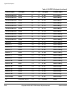
TP21 INTCLK Test clock from USB debug logic
TP22 EnRST Reset test signal (part of USB debug logic)
TP23 REFCLK1 Output fromICS525 programmable oscillator in USB debug logic
TP24 SPARE1 Test output from PLD
TP25 SPARE2 Test output from PLD
TP26 REFCLK Output fromICS525 programmable oscillator in USB debug logic
TP27 VLCD Power supply test (nominal 12V to LCD)
TP28 5VANALOG Power supply test (5V audio)
TP30 nSCIDATAEN1 SC interface enable 1
TP31 nSCIDATAEN0 SC interface enable 0
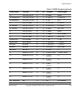
TP32 SDC_TDI JTAG test signal
TP33 PLD_TDO JTAG test signal
TP34 FPGA_TDI JTAG test signal
TP35 3V3 3.3V power supply ARM926EJ-S PXP Development Chip
TP36 1V5 1.5 V power supply to FPGA
Table A-13 Test point functions (continued)
Test point Signal Function