Hardware Description
3-12 Copyright © 2003-2007 ARM Limited. All rights reserved. ARM DUI 0224F
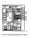
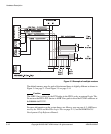
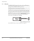
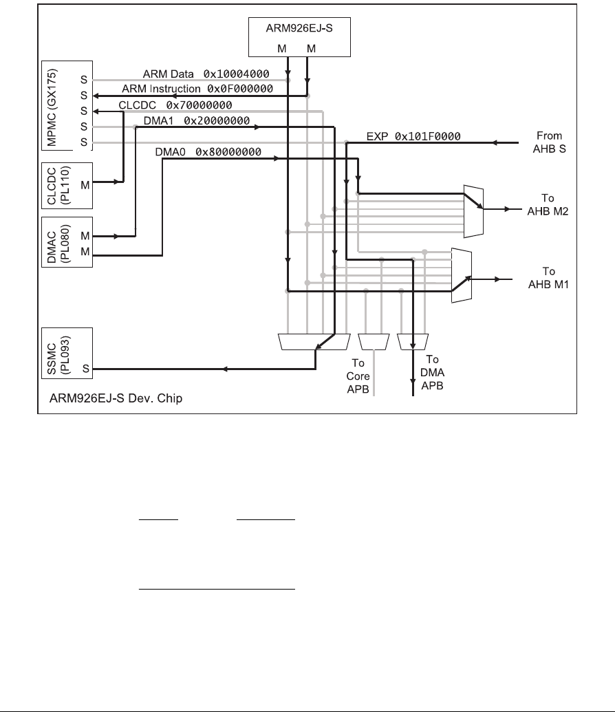
Figure 3-3 Example of multiple masters
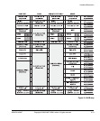
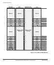
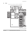
The default memory map for each of the internal buses is slightly different as shown in
Figure 3-4 on page 3-13 and Figure 3-5 on page 3-14.
Caution
The AHB S bus is driven by the PCI bridge in the FPGA or by an external Logic Tile.
Do not use the FPGA PCI master to AHB S bus path to drive the PCI M2 addresses at
0x41000000
–
0x6FFFFFFF
.
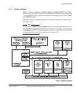
For more information on the system buses, see Memory map on page 4-3, AHB buses
used by the FPGA and RealView Logic Tiles on page F-11, and the ARM926EJ-S
Development Chip Reference Manual.


