Programmer’s Reference
4-26 Copyright © 2003-2007 ARM Limited. All rights reserved. ARM DUI 0224F
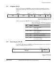
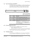
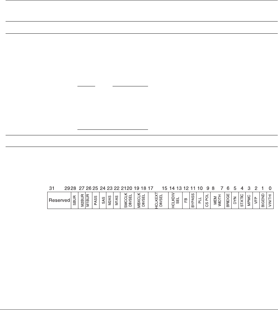
SYS_CFGDATA2 at address
0x1000002C
contains the configuration settings to apply to
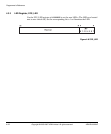
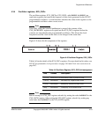
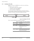
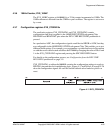
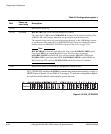
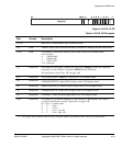
HDATA2 pins. Figure 4-12 and Table 4-9 on page 4-27 show the configuration signals
for each bit and the default value loaded at power on reset.
Figure 4-12 SYS_CFGDATA2
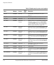
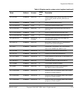
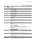
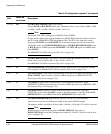
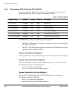
Table 4-8 Configuration register 1
Bits
Power-on
reset state
Description
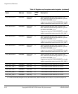
[31:24] - Reserved for future use.
[23:16]
b11110000
HCLKCTRL[7:0], clock selection multiplexors control.
The value of b1111000 selects GLOBALCLK as source for the external clocking of the
AHB M1, M2, and S bridges when they are operating in asynchronous mode.
The external bridge clocks are not used by default however, as the AHB bridges operate
in synchronous mode unless SYS_CONFIGDATA2[26:22] bits are changed from their
default values (see ARM926EJ-S PXP Development Chip clocks on page 3-39).
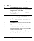
Note
HCLKCTRL[0] is read-only and reflects the state of the nGLOBALCLKEN signal
from signal Z50 on an external RealView Logic Tile: If no tile is connected,
nGLOBALCLKEN is pulled LOW by a resistor inside the PB926EJ-S FPGA and
GLOBALCLK is generated from OSC0. If nGLOBALCLKEN is pulled HIGH, the
RealView Logic Tile is driving GLOBALCLK and the local source is disabled.
[15:0] - Reserved for future use for AHB M1 configuration, should be zero.


