Hardware Description
ARM DUI 0224F Copyright © 2003-2007 ARM Limited. All rights reserved. 3-93
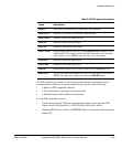
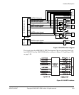
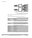
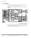
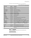
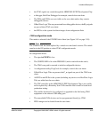
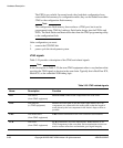
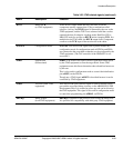
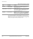
The signals associated with the USB interfaces are shown in Table 3-24.
Note
For a full description of the USB controller, refer to the datasheet for the
TransDimension OTG243.
Table 3-24 USB interface signal assignment
Signal name Direction Description
DPx Bidirectional D+ data line
DMx Bidirectional D– data line
USBETHD[31:0] Bidirectional Data lines of USB controller
USBETHA[8:2] From FPGA Address lines of USB controller
USBnCS From FPGA Controller chip select
USBnRD From FPGA Read strobe to controller
USBnWR From FPGA Write strobe to controller
USBnINT To FPGA Controller interrupt out
USBnRESET From FPGA Controller reset
USBWAKEUP From FPGA FPGA drives this signal HIGH to wake up the controller
REFCLK24MHZ2U From FPGA 24MHz reference clock to controller
nOC From OTG Over current detect (disconnects power to USB2 and USB3)
USBEOT[1:0] To FPGA DMA end of transfer. USBEOT1 for channel 1, USBEOT0 for channel 0.
USBDRQ[1:0] From FPGA DMA request. USBDRQ1 for channel 1, USBDRQ0 for channel 0.
USBDACK[1:0] To FPGA DMA acknowledge. USBDACK1 for channel 1, USBEDACK0 for
channel 0.
nEXVBO From FPGA Connects additional power to the OTG (VBUS)
VBP From FPGA Connects additional power to the OTG (VBUS)
VBUS - If the OTG is in slave mode, this is the incoming 5V digital power supply
from the cable.


