


Memory Expansion Boards
ARM DUI 0224F Copyright © 2003-2007 ARM Limited. All rights reserved. E-7
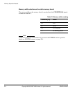
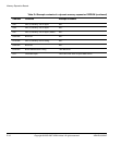
The base address of the information block is determined by the device chip select used.
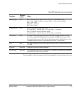
Table E-2 Chip Select information block
Function
Address
offset
Value
Memory Type
0x0
0x0 = Reserved, 0x1 = Static Disk On Chip, 0x2 = Static NOR flash,
0x3 = Static SRAM, 0x4–0x80 = Reserved, 0x81 = Single Data Rate SDRAM,
0x82 = Sync Flash,
0x83–0xFE = Reserved,
0xFF = Not fitted.
Memory Width
0x01
Bits [3:0] indicate the chip-select width:
0 = byte wide, 1 = 16-bit wide, 2 = 32-bit wide, 3 = Reserved.
Bits [7:4] indicate the device memory width:
0 = byte wide, 1 = 16-bit wide, 2 = 32-bit wide, 3 = Reserved.
Access time
0x02
Two bytes containing the access time (tach) decoded as a binary number of 100ps.
Location 2 contains the LSB and location 3 contains the MSB. For example, a flash
device with 120ns access is 1200 * 0.1ns. The decimal value is 1200 and the hex value
is
0x04B0
, therefore location 2 contains
0xb0
and location 3 contains
0x04.
Size
0x04
Four bytes containing the size of the memory in bytes location 4 is the LSB and location
7 is MSB.
Reserved
0x08–0x0F
Eight bytes reserved for future expansion
Device string
0x10–0x2F
Null terminated string of up to 32 characters (31 characters + null character) containing
the manufacturer name and part number.