


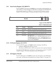
Programmer’s Reference
ARM DUI 0224F Copyright © 2003-2007 ARM Limited. All rights reserved. 4-27
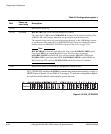
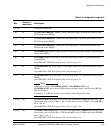
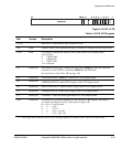
Table 4-9 Configuration register 2
Bits
Power-on
reset state
Description
[31:29] - Reserved for future use.
[28]
b0
CFGINCROVERRIDES, AMBA on-chip AHB slave bridge. Override burst transfer with
INCR mode (active HIGH).
[27]
b0
CFGINCROVERRIDEM2, AMBA off-chip AHB bridge 2. Override burst transfer with
INCR mode (active HIGH).
[26]
b0
CFGINCROVERRIDEM1, AMBA off-chip AHB bridge 1. Override burst transfer with
INCR mode (active HIGH).
[25]
b0
CFGAHBPASST, AMBA bridges. Switch the AHB M1, M2, and S bridges to pass-through
mode (active HIGH).
[24]
b0
CFGAHBSASYNC, clock control. Force the slave bridge AHB S to asynchronous mode
(active HIGH).
See ARM926EJ-S PXP Development Chip clocks on page 3-39.
[23]
b0
CFGAHBM2ASYNC, clock control. Force bridge AHB M2 to asynchronous mode (active
HIGH).
See ARM926EJ-S PXP Development Chip clocks on page 3-39.
[22]
b0
CFGAHBM1ASYNC, clock control. Force off-chip bridge 1 to asynchronous mode (active
HIGH).
See ARM926EJ-S PXP Development Chip clocks on page 3-39.
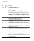
Note
If Switch S1-3 is ON, CFGAHBM1ASYNC, CFGAHBM2ASYNC, and
CFGAHBSASYNC are all forced HIGH and asynchronous mode is used for the AHB M1,
M2, and S bridges.
If Switch S1-3 is OFF, the mode for each bridge is selected by the bit value.
[21:20]
b01
CFGSMCCLKDIVSEL[1:0], clock control. Sets the HCLK to SMCLK divide ratio. The
divide value is set as follows:
b00
= 1
b01
= 2 (The default clock is 35MHz, one half HCLK.)
b10
= 3
b11
= 4
See ARM926EJ-S PXP Development Chip clocks on page 3-39.
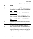
[19:18]
b00
CFGMBXCLKDIVSEL[1:0], clock control. Sets the HCLK to MBXCLK divide ratio. The
divide value is set as follows:
b00
= 1 (The default MBX clock is 70MHz, the same as HCLK.)
b01
= 2
b10
= 3
b11
= 4
See ARM926EJ-S PXP Development Chip clocks on page 3-39.