


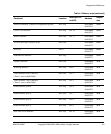


Programmer’s Reference
ARM DUI 0224F Copyright © 2003-2007 ARM Limited. All rights reserved. 4-9
4.2 Configuration and initialization
This section describes how the ARM926EJ-S PXP Development Chip and external
memory and peripherals are configured and initialized at power on. See Status and
system control registers on page 4-17 and Boot Select Register, SYS_BOOTCS on
page 4-34 for details on configuration operations that can be performed after the system
has started. See also Configuration control on page 3-7 and Configuration registers
SYS_CFGDATAx on page 4-25.
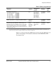
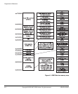
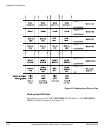
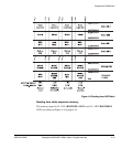
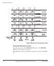
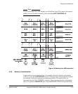
4.2.1 Remapping of boot memory
On reset, the ARM926EJ-S PXP Development Chip begins executing code at address
0x0
. This address is normally volatile SDRAM. Remapping allows non-volatile static
memory to be decoded for accesses to low memory. Remapping of non-volatile memory
to the boot region at
0x00000000
–
0x03FFFFFF
is done by the following signals:
BOOTCSSEL[1:0]
These signals (from configuration switches S1-1 and S1-2) select the
non-volatile memory to use if remapping is active (DEVCHIP REMAP
HIGH).
DEVCHIP REMAP
This signal (from the System Controller register at
0x101E0000
) in the
ARM926EJ-S PXP Development Chip redirects accesses to memory
region
0x00000000
–
0x03FFFFFF
(normally decoded to dynamic chip select
0) to either static chip select 1 to non-volatile memory.
Depending on the state of BOOTSEL[1:0], the non-volatile memory
used for boot memory can be either NOR flash, or Disk-on-Chip, static
expansion memory on a memory expansion board, or memory on a
RealView Logic Tile. At reset, the DEVCHIP REMAP signal is HIGH.
FPGA_REMAP
This signal (from the SYS_MISC register in the FPGA) redirects chip
select 3 (normally
0x34000000
–
0x37FFFFFF
) to one of Disk-on-Chip
(
0x30000000
), NOR flash (
0x34000000
), or static expansion memory
(
0x3C000000
) depending on the state of BOOTCSSEL[1:0]. At reset, the
FPGA_REMAP signal is HIGH.