Hardware Description
3-54 Copyright © 2003-2007 ARM Limited. All rights reserved. ARM DUI 0224F
3.5.3 Peripheral clocks
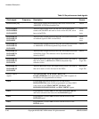
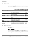
Table 3-11 lists the other memory and peripheral clocks on the PB926EJ-S.
For more detail on the clocking system, see the files in the
Schematics
directory of the
CD supplied with the PB926EJ-S.
3.5.4 Clock multiplexor logic
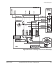
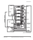
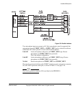
Figure 3-23 on page 3-55 shows the clock multiplexor switches and the effect of the
HCLKCTRL[4:0] signals.
Note
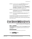
The HCLKx_L2S and HCLKx_L2F clocks must be driven from the same reference
source in the RealView Logic Tile. The HCLKx_F2S and HCLKx_F2F clocks are
driven from the same source in the PB926EJ-S FPGA. Two signals are used for each
clock for loading purposes and to allow for future expansion.
Table 3-11 PB926EJ-S clocks and clock control signals
Clock signal Frequency Description Source
AACIBITCLK 12.288MHz This is the synchronization clock from the audio CODEC. The
clock is an input to the AACI PrimeCell.
Crystal
oscillator
CLCDCLKEXT 6–50MHz The clock for PL110 CLCD Controller in the development chip
can be derived from this input.
ICS307
OSC4
ETHLCLK AHB M2 ETHLCLK is used to synchronize data transfers between the
external controller and the FPGA. (The Ethernet controller uses a
25MHz crystal for clocking signals to and from the Ethernet
connector.)
HCLKM2
(typically
OSC0)
MPMCCLK[4:0] - The dynamic memory clocks from the MPMC in the development
chip. This is a buffered version of HCLK.
MPMC
controller
PCICLK - This is the clock from the PCI backplane.
SCIREFCLKEXT 24MHz The clock for PL131 SCI in the development chip can be derived
from this input. This is a buffered version of REFCLK24MHZ.
24MHz
reference
SMCLK[2:0] - The static memory clocks from the SSMC in the development
chip. This is HCLK divided by 1, 2, or 3.
SSMC
controller


