


Signal Descriptions
A-36 Copyright © 2003-2007 ARM Limited. All rights reserved. ARM DUI 0224F
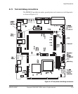
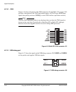
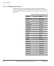
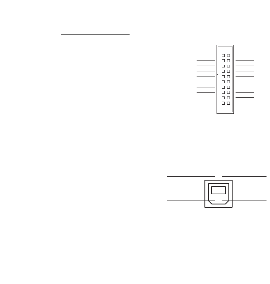
A.13.2 JTAG
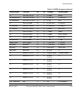
Figure A-16 shows the pinout of the JTAG connector J31 and Table 3-25 on page 3-98
provides a description of the JTAG and related signals. All JTAG active HIGH input
signals have pull-up resistors (DGBRQ is active LOW and has a pull-down resistor).
Note
The term JTAG equipment refers to any hardware that can drive the JTAG signals to
devices in the scan chain. Typically this is RealView ICE or Multi-ICE, although
hardware from other suppliers can also be used to debug ARM processors.
Figure A-16 Multi-ICE JTAG connector J31
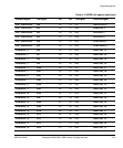
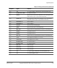
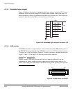
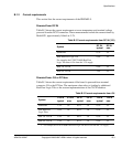
A.13.3 USB debug port
Figure A-17 shows the signals on the USB debug connector J30. USBDP and USBDM
are the positive and negative USB data signals.
Figure A-17 USB debug connector J30
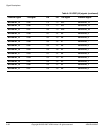
3V33V3
GND
GND
GND
GND
GND
GND
GND
GND
GND
nTRST
TDI
TMS
TCK
RTCK
TDO
nSRST
DBGRQ
DBGACK
1
19
2
20
2 USBDM
3 USBDP
VCC 1
GND 4