Programmer’s Reference
ARM DUI 0224F Copyright © 2003-2007 ARM Limited. All rights reserved. 4-17
4.3 Status and system control registers
The PB926EJ-S status and system control registers enable the processor to determine
its environment and to control some on-board operations. The registers, listed in
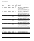
Table 4-4 on page 4-18, are located from
0x10000000
.
See also the ARM PrimeCell System Controller (SP810) Technical Reference Manual
for details of control registers in the SP810 System Controller that is in the
ARM926EJ-S PXP Development Chip. See also Reset controller on page 3-22 for a
description of the reset logic.
Note
All registers are 32 bits wide and do not support byte writes. Write operations must be
word-wide. Bits marked as reserved in the following sections must be preserved using
read-modify-write operations.
In Table 4-4 on page 4-18, the entry for Reset Level indicates the highest reset level that
modifies its contents:
Level 6 This a programmable reset level that is triggered by a software reset,
nSRST, P_nRST, or nPBRESET. See Reset controller on page 3-22 for
a description of programmable reset levels and the reset signals.
Level 2 Pressing the SDC RECONFIG button drives the nPBSDCRECONFIG
signal active and initiates reconfiguration. The registers are loaded from
a writable configuration register. For example, configuration loads the
OSC0 clock values from SYS_OSCRESET0. This allows the clock to be
changed for testing new divider values. A hard reset of level 0 resets both
the OSC0 and SYS_OSCRESET0 registers to the hard-wired default
values.
Level 1 Pressing the FPGA CONFIG initiates reconfiguration of the FPGA.
Level 0 The system power on reset (nSYSPOR) is a level 0 reset and initializes
all registers to their default value.


