


Hardware Description
ARM DUI 0224F Copyright © 2003-2007 ARM Limited. All rights reserved. 3-51
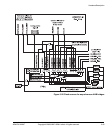
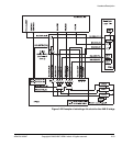
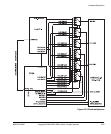
In the power-saving modes, an external low-frequency clock is used as CPUCLK. If
the AHB bridges operated synchronous mode, the resulting timing for the external part
of the AHB bridge would be CPUCLK divided by the values used for HCLKDIV and
HCLKEXTDIV and the bus would be extremely slow. Therefore, the AHB bridges
must operate in asynchronous mode and the bus timing is controlled by external clocks
HCLKM1, HCLKM2, and HCLKS.
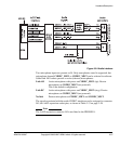
The following signals control the PLL usage:
CFGPLLBYPASS If HIGH, the PLL is bypassed and XTALCLKEXT is the input to
the CPUCLK multiplexor. The signal is controlled by the value
of bit 11 of the SYS_CONFIGDATA2 register. The default is
LOW and the PLL output is used.
CFGUSEPLL If LOW, an external clock (REFCLK32K, PLLCLKEXT, or
XTALCLKEXT) is used instead of the PLL output as CPUCLK.
The signal is controlled by the value of bit 10 of the
SYS_CONFIGDATA2 register. The default is HIGH and the
output from the PLL is used and the power-saving modes are
disabled.
By default, HCLKM1, HCLKM2, and HCLKS are driven from GLOBALCLK.
(GLOBALCLK is by default operating at OSC0 frequency.) For details on changing
the AHB asynchronous bridge clock frequencies, see Operating the AHB bridges in
asynchronous mode on page 3-44.
Peripheral clocks
The UART, Smart Card Interface, and Synchronous Serial Port in the ARM926EJ-S
PXP Development Chip are clocked from a 24MHz reference clock from the FPGA.
The clock is a buffered version of the REFCLK24MHZ (from the crystal oscillator
circuit that is part of OSC0).
The Dual Timer Counter modules in the ARM926EJ-S PXP Development Chip are
clocked by a 1MHz reference clock from the FPGA. The 1MHz clock is generated by
dividing the 24MHz reference by 24 in the FPGA.