


Programmer’s Reference
4-48 Copyright © 2003-2007 ARM Limited. All rights reserved. ARM DUI 0224F
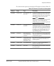
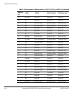
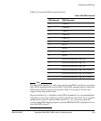
4.7.1 PrimeCell Modifications
The register map for the variant of the PL110 used in the ARM926EJ-S PXP
Development Chip is not the same as that listed for the standard PL110. The differences
are listed in Table 4-28.
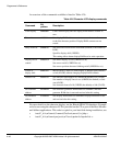
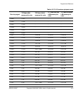
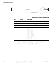
4.7.2 Display resolutions and display memory organization
Different display resolutions require different data and synchronization timing. Use
registers CLCD_TIM0, CLCD_TIM1, CLCD_TIM2, and SYS_OSCCLK4 to define
the display timings. Table 4-29 lists the register and clock values for different display
resolutions.
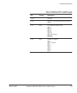
Table 4-28 PrimeCell CLCDC register differences
Address
(Dev.
Chip)
Reset value
(Dev. Chip)
Description in PL110
TRM
Difference
0x10120018 0x0
LCDControl, LCD panel
pixel parameters
CLCDC TRM lists address as
0x1012001C
0x1012001C 0x0
LCDIMSC, interrupt mask
set and clear
CLCDC TRM lists address as
0x10120018
0x10120800–
0x10120C2C
0x0
Not present Hardware cursor registers from PL111 (see the
ARM926EJ-S Technical Reference Manual for details)
0x10120FE0 0x93
CLCDPeriphID0 CLCDC TRM lists value as
0x10
0x10120FE4 0x10
CLCDPeriphID1 CLCDC TRM lists value as
0x11
Table 4-29 Values for different display resolutions
Display resolution
CLCDCLK frequency
and SYS_OSCCLK4
register value
CLCD_TIM0
register at
0x10120000
CLCD_TIM1
register
0x10120004
CLCD_TIM2
register at
0x10120008
QVGA(240x320) (portrait) on VGA 25MHz,
0x2C77 0xC7A7BF38 0x595B613F 0x04eF1800
QVGA (320x240) (landscape) on
VGA
25MHz,
0x2C77 0x9F7FBF4C 0x818360eF 0x053F1800
QCIF (176x220) (portrait) on VGA 25MHz,
0x2C77 0xe7C7BF28 0x8B8D60DB 0x04AF1800
VGA (640x480) on VGA 25MHz,
0x2C77 0x3F1F3F9C 0x090B61DF 0x067F1800