


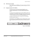
Programmer’s Reference
ARM DUI 0224F Copyright © 2003-2007 ARM Limited. All rights reserved. 4-33
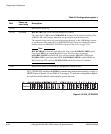
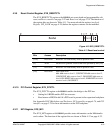
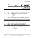
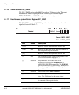
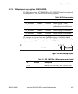
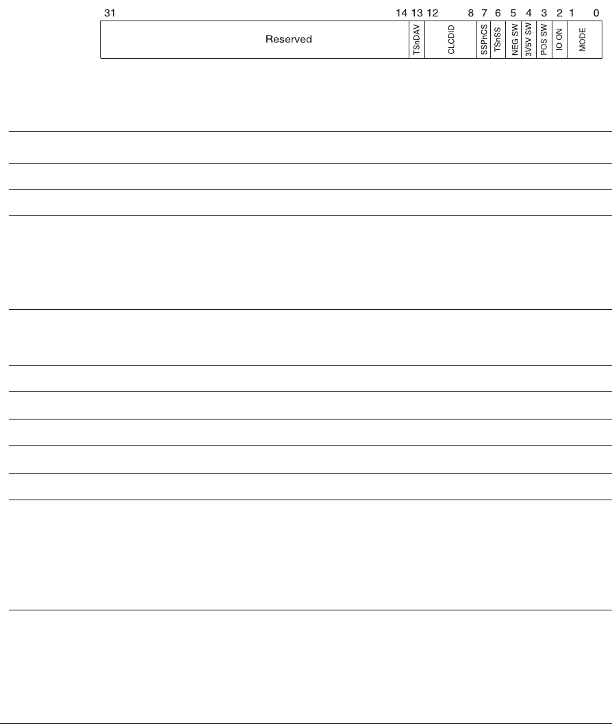
Figure 4-15 SYS_CLCD
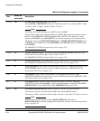
Table 4-14 SYS_CLCD register
Bits Access Description
[31:14] - Reserved. Use read-modify-write to preserve value.
[13] Read TSnDAV status, LOW indicates that data is available for reading from the touchscreen.
[12:8] Read CLCDID[4:0], returns the setting of the ID links on the CLCD adaptor board
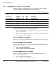
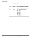
Value Display
0 320x240 QVGA
1 640x480 VGA
2 220x176 QCIF
3-31 Reserved
[7] Read/write SSP expansion chip select. If HIGH, the chip select (SSPnCS) on the SSP expansion
connector is active. SSPCS is inverted to SSPnCS at the FPGA pin.
See Synchronous Serial Port, SSP on page 3-84.
[6] Read/write Touchscreen enable (TSnSS) to controller on CLCD adaptor board
[5] Read/write
VDDNEGSWITCH
a
, enable NEG voltage on the CLCD adaptor board
a. The voltage control selection in the SYS_CLCD register might be overridden by links on the CLCD adaptor board.
[4] Read/write
PWR3V5VSWITCH
a
, enable FIXED voltage on the CLCD adaptor board
[3] Read/write
VDDPOSSWITCH
a
, enable POS voltage on the CLCD adaptor board
[2] Read/write
LCDIOON
a
, enable the RGB signal buffers on CLCD adaptor board
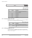
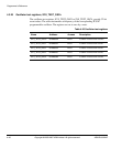
[1:0] Read/write LCD Mode [1:0], controls mapping of video memory to RGB signals. See Display
resolutions and display memory organization on page 4-48.
Bit 1 Bit 0 Display mode
0 0 8:8:8
0 1 5:5:5:1
1 0 5:6:5, red LSB
1 1 5:6:5, blue LSB