Programmer’s Reference
4-16 Copyright © 2003-2007 ARM Limited. All rights reserved. ARM DUI 0224F
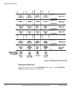
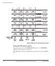
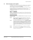
when nPBSDCRECONFIG is asserted by pressing the DEV CHIP RECONFIG
pushbutton. See Configuration from the DEV CHIP RECONFIG pushbutton on
page 3-9 for details of the CONFIGDATA signals.
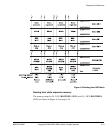
The values in the SYS_CFGDATAx registers retain their value during the ARM926EJ-S
PXP Development Chip reconfiguration. The DEV CHIP RECONFIG pushbutton can
therefore be used to test different configuration options without resetting the system.
See Configuration registers SYS_CFGDATAx on page 4-25 for details of the power-on
default values.
See also the ARM Multiport Memory Controller (GL175) Technical Reference Manual
and the ARM PrimeCell Static Memory Controller (PL093) Technical Reference
Manual for detailed information on the memory controllers.
Memory banks
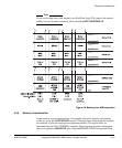
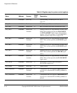
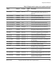
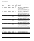
Table 4-3 lists the controller memory banks, chip selects, and memory range.
Table 4-3 Memory chip selects and address range
Bank Chip select Address range Device
MPMC bank 4 nMPMCDYCS0
0x00000000–0x07FFFFFF
SDRAM
MPMC bank 5 nMPMCDYCS1
0x08000000–0x0FFFFFFF
Expansion dynamic memory
MPMC bank 6 nMPMCDYCS2
0x70000000–0x77FFFFFF
Expansion dynamic memory
MPMC bank 7 nMPMCDYCS3
0x78000000–0x7FFFFFFF
Expansion dynamic memory
SSMC bank 0 nSTATICCS0
0x30000000–0x33FFFFFF
Disk-on-Chip
SSMC bank 7 nSTATICCS1
0x34000000–0x37FFFFFF
NOR flash
SSMC bank 3 nSTATICCS2
0x38000000–0x3BFFFFFF
SRAM
SSMC bank 1 nSTATICCS3
0x3C000000–0x3FFFFFFF
Expansion static memory
SSMC bank 4 nSTATICCS4
0x20000000–0x23FFFFFF
Expansion static memory
SSMC bank 5 nSTATICCS5
0x24000000–0x27FFFFFF
Expansion static memory
SSMC bank 6 nSTATICCS6
0x28000000–0x2BFFFFFF
Expansion static memory
SSMC bank 1 nSTATICCS7
0x2C000000–0x2FFFFFFF
Expansion static memory


