


Programmer’s Reference
ARM DUI 0224F Copyright © 2003-2007 ARM Limited. All rights reserved. 4-3
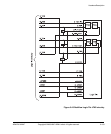
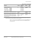
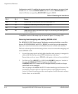
4.1 Memory map
The locations for memory, peripherals, and controllers are listed in Table 4-1 and ARM
Data bus memory map on page 4-8.
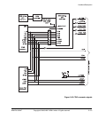
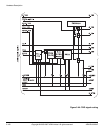
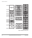
There are multiple buses in the ARM926EJ-S PXP Development Chip. Not all of the
buses can access all of the memory regions. See AHB bridges and the bus matrix on
page 3-10 and the ARM926EJ-S Reference Manual for details on the bus matrix and bus
accesses.
Note
The MOVE and VFP coprocessors are not memory-mapped peripherals so they do not
appear in the memory map listed in Table 4-1. See the appropriate technical reference
manual for more detail on these devices.
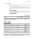
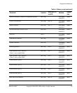
Table 4-1 Memory map
Peripheral Location
Interrupt
a
PIC
and SIC
Address
Region
size
MPMC Chip Select 0. Normally the bottom 64MB of the
first bank of SDRAM (During boot remapping, this can be
NOR flash, Disk-on-Chip, or memory on a RealView
Logic Tile.)
Note
Interrupts are for Disk-on-Chip only.
Board PIC21, SIC21
0x00000000–
0x03FFFFFF
64MB
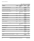
MPMC Chip Select 0, top 64MB of the first bank of
SDRAM
Board -
0x04000000–
0x07FFFFFF
64MB
MPMC Chip Select 1, dynamic expansion memory Memory
expansion
-
0x08000000–
0x0FFFFFFF
128MB
System registers FPGA -
0x10000000–
0x10000FFF
4KB
PCI controller configuration registers FPGA -
0x10001000–
0x10001FFF
4KB
Serial Bus Interface FPGA -
0x10002000–
0x10002FFF
4KB