Introduction
1-4 Copyright © 2003-2007 ARM Limited. All rights reserved. ARM DUI 0224F
1.2 PB926EJ-S architecture
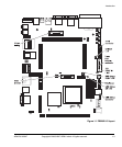
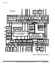
The major components on the platform are:
• ARM926EJ-S PXP Development Chip equipped with:
— ARM926EJ-S processor that supports 32-bit ARM and 16-bit Thumb
instructions sets and includes features for direct execution of Java byte
codes. Executing Java byte codes requires the Java Technology Enabling
Kit (JTEK)
— Tightly-Coupled Memory (TCM) for code (32KB) and data (32KB)
— cache memory for code (32KB) and data (32KB)
— Memory Management Unit (MMU)
— Multi-layer bus matrix that gives highly efficient simultaneous transfers
—MOVE
™
video encoding coprocessor
— MBX graphics accelerator
— Multi-Port Memory Controller (MPMC) for direct connection to dynamic
memory
— Synchronous Static Memory Controller (SSMC) for direct connection to
static (SRAM or flash) memory
— VFP9 Vector Floating Point coprocessor
— two external AHB master bridges and one external AHB slave bridge
— AHB monitor for detailed analysis of bus activity
— System Controller
— DMA controller
— Vectored Interrupt Controller (VIC)
— Color LCD controller (CLCDC)
— Three UARTs,
— Synchronous Serial Port (SSP)
— Smart Card Interface (SCI)
— Four eight-bit GPIOs
— Real Time Clock (RTC)
— Two programmable timers
— Watchdog timer
— Embedded Trace Macrocell (ETM9)
— Embedded-ICE logic for JTAG debugging
— Phase-Locked Loop (PLL)
— Configuration Block.


