


Programmer’s Reference
4-94 Copyright © 2003-2007 ARM Limited. All rights reserved. ARM DUI 0224F
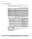
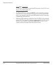
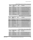
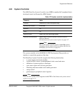
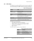
+0x6c SMBWSTOENR3
0x0
Output Enable Assertion Delay 3
+0x70 SMBWSTWENR3
0x1
Write Enable Assertion Delay 3
+0x74 SMBCR3
0x303021
Control Register for memory bank 3
+0x7c SMBWSTBRDR3
0x0
Burst Read Wait state Control Reg 3
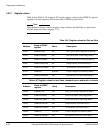
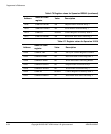
Table 4-71 Register values for Spansion LV256
Address
Name of SSMC
register
Value Description
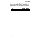
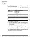
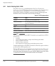
+0x80 SMBIDCYR4
0x0
Idle Cycle Control Register for bank 4
+0x84 SMBWSTRDR4
0x4
Read Wait State Control Reg bank 4
+0x88 SMBWSTWRR4
0x3
Write Wait State Control Reg Bank 4
+0x8c SMBWSTOENR4
0x1
Output Enable Assertion Delay 4
+0x90 SMBWSTWENR4
0x1
Write Enable Assertion Delay 4
+0x94 SMBCR4
0x303121
Control Register for memory bank 4
+0x9c SMBWSTBRDR4
0x1
Burst Read Wait state Control Reg 4
Table 4-70 Register values for Spansion BDS640 (continued)
Address
Name of SSMC
register
Value Description