


Programmer’s Reference
ARM DUI 0224F Copyright © 2003-2007 ARM Limited. All rights reserved. 4-35
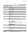
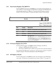
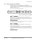
Figure 4-17 SYS_BOOTCS
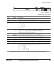
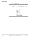
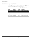
Table 4-16 BOOT configuration switches
Bits Access Description
[31:8] - Reserved. Use read-modify-write to preserve value.
[7] Read Stack image (RealView Logic Tile image 0 or 1). The default is tile image 0 (S1-8
OFF).
[6:5] Read FPGA image to load on power on.
b00 Image 0 (default, S1-7 and S1-6 OFF)
b01 Image 1
b10 Image 2
b11 Image 3
[4] Read Low-frequency startup mode. If 1, OSCCLC0 is programmed to generate a 10MHz
reference clock instead of a 35MHz reference. The default is 0 (S1-5 OFF).
[3] Read Reserved. S1-4 must be set to 0 (OFF)
[2] Read If 1, the AHB bus bridge operates in asynchronous mode instead of synchronous
mode. The default is 0 (S1-3 OFF).
[1:0] Read Static boot memory select switches (S1-2 and S1-1)
b00 Disk-on-chip
b01 NOR flash (default setting)
b10 Static expansion memory
b11 AHB expansion memory