


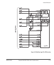

Hardware Description
3-98 Copyright © 2003-2007 ARM Limited. All rights reserved. ARM DUI 0224F
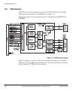
The FPGAs are volatile. In normal mode, they load their configuration from
nonvolatile flash memory. In configuration mode, they can be loaded from either
JTAG or the configuration flash memory.
Note
The configuration flash memory does not have a JTAG port, but it can be
programmed using JTAG by loading a flash-loader design into the FPGAs and
PLDs. The flash-loader can then transfer data from the JTAG programming utility
to the configuration flash.
After configuration you must:
1. remove the CONFIG link
2. power cycle the development system.
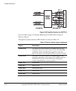
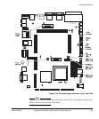
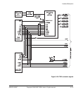
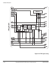
JTAG signals
Table 3-25 provides a description of the JTAG and related signals.
Note
In the description in Table 3-25, the term JTAG equipment refers to any hardware that
can drive the JTAG signals to devices in the scan chain. Typically this is RealView ICE,
Multi-ICE, or the embedded USB debug logic.
Table 3-25 JTAG related signals
Name Description Function
TDI Test data in
(from JTAG equipment)
TDI and TDO connect each component in the scan chain.
TDO Test data out
(to JTAG equipment)
TDO is the return path of the data input signal TDI. The JTAG
components are connected in the return path so that the length of
track driven by the last component in the chain is kept as short as
possible.
TMS Test mode select
(from JTAG equipment)
TMS controls transitions in the TAP controller state machine.
TCK Test clock
(from JTAG equipment)
TCK synchronizes all JTAG transactions. TCK connects to all
JTAG components in the scan chain. Series termination resistors are
used to reduce reflections and maintain good signal integrity.