RealView Logic Tile
ARM DUI 0224F Copyright © 2003-2007 ARM Limited. All rights reserved. F-7
F.3.4 RealView Logic Tile clocks
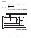
The PB926EJ-S can receive the global clock or transmit the global clock to all of the
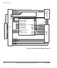
boards in the RealView Logic Tile stack. Table F-1 on page F-8 lists the RealView
Logic Tile clocks. Also, the clock multiplexor can select clock signals from the
RealView Logic Tiles as the source for the M1, M2, and S clocks.
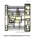
The CLK_GLOBAL signal is present on all RealView Logic Tiles. The signal goes to
the CLK_GLOBAL_INinput of the FPGAs on the tiles.
The FPGA on each tile outputs a CLK_GLOBAL_OUT signal to a tristate buffer. If
the tile signal CLK_GLOBAL_OUT_nEN is LOW, the local tile signal
CLK_GLOBAL_OUT becomes the global clock for the system.
Caution
If the tile signal CLK_GLOBAL_OUT_nEN is LOW, the RealView Logic Tile drives
the CLK_GLOBAL signal. Ensure that nGLOBALCLKEN (signal Z50 on the
RealView Logic Tile) is driven HIGH to disable the clock driver on the PB926EJ-S:
•If CLK_GLOBAL_OUT_nEN is HIGH and Z50 is LOW, both the RealView
Logic Tile and PB926EJ-S sources for CLK_GLOBAL are disabled and there
will not be a clock signal present on CLK_GLOBAL.
•If CLK_GLOBAL_OUT_nEN is LOW and Z50 is LOW, both the RealView
Logic Tile and PB926EJ-S sources for CLK_GLOBAL are enabled and the two
CLK_GLOBAL signals will conflict.
OSCCLK0 from OSC0 on the PB926EJ-S is the default reference clock for
XTALCLKDRV. XTALCLKDRV is normally used as the source for the Logic Tile
CLK_GLOBAL signal and for the PB926EJ-S GLOBALCLK, external AHB bridge
clocks, and the PLL reference CPUCLK signals.
The M1, M2, and S clocks for the FPGA and the development chip are selected by the
multiplexing circuitry described in Operating the AHB bridges in asynchronous mode
on page 3-44.
Note
Some of the standard RealView Logic Tile clocks, CLK_NEG_DN_IN for example,
are not used.
Also some clocks that are inputs to the bus clock multiplexors, HCLKM1L2F for
example, are not normally clock outputs on the RealView Logic Tile.


