


Programmer’s Reference
ARM DUI 0224F Copyright © 2003-2007 ARM Limited. All rights reserved. 4-49
The mapping of the 32 bits of pixel data in memory to the RGB display signals depends
on the resolution and display mode. Table 4-30 lists software usage of memory bits and
Table 4-31 on page 4-51 lists the correspondence between the hardware pins and the
bits in memory.
Note
For resolutions based on 16 bits per pixel, two pixels (pixel0 and pixel1) are encoded in
one 32-bit word.
Rx, Gx, and Bx in Table 4-30 and Table 4-31 on page 4-51 refer to bits used to set the
red, green, and blue brightness.
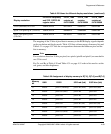
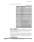
SVGA (800x600) on SVGA 36MHz,
0x2CAC 0x1313A4C4 0x0505F657 0x071F1800
Epson 2.2in panel QCIF (176x220) 10MHz,
0x2C2A 0x00000128 0x000000DB 0x04AF1800
Sanyo 3.8in panel QVGA
(320x240)
10MHz,
0x2C2A 0x0505054C 0x050514EF 0x053F1800
Table 4-29 Values for different display resolutions (continued)
Display resolution
CLCDCLK frequency
and SYS_OSCCLK4
register value
CLCD_TIM0
register at
0x10120000
CLCD_TIM1
register
0x10120004
CLCD_TIM2
register at
0x10120008
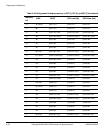
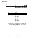
Table 4-30 Assignment of display memory to R[7:0], G[7:0], and B[7:0]
Memory
bit
8/8/8 1/5/5/5 5/6/5 red (lsb) 5/6/5 blue (lsb)
31 unused pixel1 I (intensity) pixel1 B5 (msb) pixel1 R5 (msb)
30 unused pixel1 B5 (msb) pixel1 B4 pixel1 R4
29 unused pixel1 B4 pixel1 B3 pixel1 R3
28 unused pixel1 B3 pixel1 B2 pixel1 R2
27 unused pixel1 B2 pixel1 B1 (lsb) pixel1 R1 (lsb)
26 unused pixel1 B1 (lsb) pixel1 G5 (msb) pixel1 G5 (msb)
25 unused pixel1 G5 (msb) pixel1 G4 pixel1 G4
24 unused pixel1 G4 pixel1 G3 pixel1 G3