


Signal Descriptions
ARM DUI 0224F Copyright © 2003-2007 ARM Limited. All rights reserved. A-3
A.2 Smart Card interface
The PB926EJ-S contains two Smart Card SIM sockets:
• J48 for SIM 0 (J25 uses an alternate layout for SIM 0 and is not fitted)
• J49 for SIM1 (J26 uses an alternate layout for SIM 0 and is not fitted).
Sockets J48 and J49 include a switch for card detection.
The signals on the SIM sockets are also connected to the SCI expansion socket. The
signals associated with the SCI are shown in Table A-2.
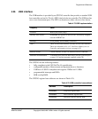
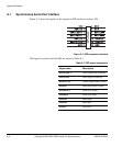
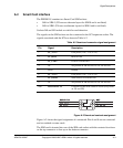
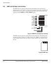
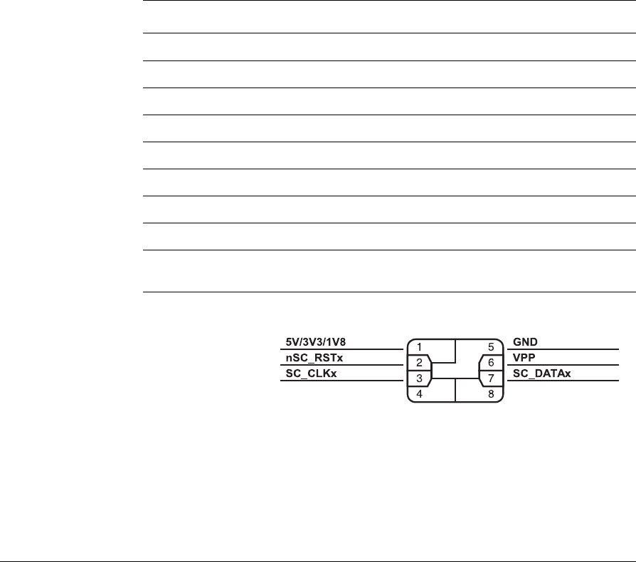
Figure A-2 Smartcard contacts assignment
Figure A-2 shows the signal assignment of a smartcard. Pins 4 and 8 are not connected
and are omitted on some cards.
The SIM card is inserted into one of the SIM card sockets with the contacts face down
on the top connector or face up on the bottom connector.
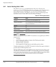
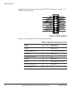
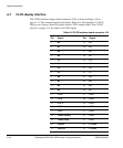
Table A-2 Smartcard connector signal assignment
Pin Signal Description
1 SC_VCCx Card power (1.8V, 3.3V, or 5V)
2 SC_RSTx Reset to card
3 SC_CLKx Clock to or from card
4 NC Not present on J48 and J49, NC on J25 and J26.
5 GND Ground
6 SC_VCCx Card power (1.8V, 3.3V, or 5V)
7 SC_DATAx Serial data to or from the card
8 NC Not present on J48 and J49, NC on J25 and J26.
SW1 nSCIDETECTx Card detect signal from switch in socket (not present
on J25 and J26)