


Introduction
ARM DUI 0224F Copyright © 2003-2007 ARM Limited. All rights reserved. 1-5
• Field Programmable Gate-Array (FPGA) that implements:
— SSP, Smart Card, two MMC/SD card, UART, and two KMI controllers
— configuration registers
— interface to onboard Ethernet controllers
— interface to onboard audio CODEC
— interface to onboard On-the-Go (OTG) USB controller (three connectors)
— registers for status, ID, onboard switches, LEDs, and clock control
— a secondary interrupt controller and external DMA control logic
— interface to PCI bus (for expansion through optional PCI expansion
enclosure).
• 128MB of 32-bit wide SDRAM
• 2MB of 32-bit wide static RAM
• 64MB of 32-bit wide NOR flash
• 64MB of 16-bit wide NAND Disk-on-Chip flash
• up to 320MB of static memory in an optional static memory expansion board
• up to 256MB of SDRAM in an optional dynamic memory expansion board
• programmable clock generators
• connectors for VGA, color LCD display interface board, PCI, UART, GPIO,
keyboard, mouse, Smart Card, USB, audio, MMC, SSP, and Ethernet
• RealView Logic Tile connector (one or more optional RealView Logic Tiles can
be used to develop custom IP)
• debug and test connectors for JTAG, AHB monitor, ChipScope, and Trace port
• DIP switches and LEDs
• 2 row by 16 character LCD display
• power conversion circuitry
• Real-Time Clock (RTC)
• time of year clock with backup battery.
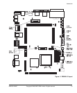
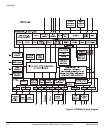
1.2.1 System architecture
Figure 1-2 on page 1-6 shows the architecture of the PB926EJ-S.