


Hardware Description
ARM DUI 0224F Copyright © 2003-2007 ARM Limited. All rights reserved. 3-41
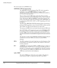
Default operation
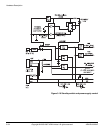
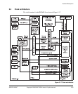
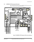
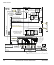
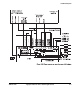
Figure 3-19 on page 3-42 shows a simplified block diagram with default clock settings
and the internal and external multiplexors replaced by an equivalent circuit.
Caution
It is recommended that you use the default value of
0xE0
for the clock multiplexing
signals HCLKCTRL[7:0]. Changing the value of HCLKCTRL[7:0] is only required
if you want to individually control the source for XTALCLKEXT (GLOBALCLK),
AHB M1, AHB M2, or AHB S.
If you install a Logic Tile for example, you can add additional clock generation and
control logic in the tile FPGA. If you change the multiplexing signals, ensure that you
have programmed the oscillators to generate the correct bridge frequencies or have
implemented the correct clock generation logic in your RealView Logic Tile.
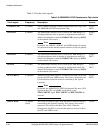
Peripheral clocks 24MHz and
1MHz
The SSP, SCI, and UART use an external 24MHz as reference. The
timers use an external 1MHZ clock as reference.
24MHz
crystal
XTALCLKDRV 6–75MHz For the default clock multiplexor setting, this signal is driven from
the FPGA (from OSC0) and is distributed as HCLKM1,
HCLKM2, HCLKS, PLLCLKEXT, GLOBALCLK, and
XTALCLKEXT.
ICS307
OSC0
XTALCLKEXT 6–75MHz When the ARM926EJ-S PXP Development Chip PLL is used, this
input is used as the reference clock for the PLL. When the on-chip
PLL is not used this input can be used as the reference clock for the
CPU and AMBA clocks. This clock is selected by the Clock and
Reset Controller which is controlled by the System Controller.
ICS307
OSC0
Table 3-5 ARM926EJ-S PXP Development Chip clocks (continued)
Clock signal Frequency Description Source