


Programmer’s Reference
4-28 Copyright © 2003-2007 ARM Limited. All rights reserved. ARM DUI 0224F
[17:15]
b001
CFGHCLKEXTDIVSEL[2:0], clock control.
Sets the HCLK to HCLKEXT divide ratio. The divide value is set as follows:
b000
= 1
b001
= 2
b010
= 3
b011
= 4
b100
= 5
b101
= 6
b110
= 7
b111
= 8
Note
The default SYS_OSC0 setting gives an OSC0 clock of 35MHz.
For the default values of the system multiplexors, OSCCLK0 provides the reference clock to
the PLL in the ARM926EJ-S PXP Development Chip. The PLL clock adjusts its output
frequency (CPUCLK) so that HCLKEXT is at the same frequency as the reference clock.
The default values for CFGHCLKDIVSEL[1:0] and CFGHCLKEXTDIVSEL[2:0] result
in HCLK equal to 70MHz (two times HCLKEXT) and CPUCLK equal to 210MHz (three
times HCLK).
See ARM926EJ-S PXP Development Chip clocks on page 3-39.
[14:13]
b10
CFGHCLKDIVSEL[1:0], clock control. Sets the CPUCLK to HCLK divide ratio. The
divide value is set as follows:
b00
= 1
b01
= 2
b10
= 3
b11
= 4
See ARM926EJ-S PXP Development Chip clocks on page 3-39.
[12]
b0
CFGPLLSHORTFB, clock control (active HIGH). Removes the clock tree delay from the
PLL feedback (see ARM926EJ-S PXP Development Chip clocks on page 3-39).
[11]
b0
CFGPLLBYPASS, clock control (active HIGH). Forces the PLL output to be bypassed. The
XTALCLKEXT signal is used to clock the AMBA subsystem (see ARM926EJ-S PXP
Development Chip clocks on page 3-39).
[10]
b1
CFGUSEPLL, clock control (active HIGH). Uses the output from the PLL in the
ARM926EJ-S PXP Development Chip to clock the AMBA subsystem (see ARM926EJ-S PXP
Development Chip clocks on page 3-39).
[9]
b0
CFGBOOTCSPOL, memory control. Defines the polarity of the static chip select
STATICCS1 at reset when the MPMC is used as the static memory controller. When HIGH,
nMPMCSTCS1 is active HIGH.When LOW, nMPMCSTCS1 is active LOW.
[8:7]
b10
CFGBOOTMEMWIDTH[1:0], memory width for STATICCS1 from the SSMC.
These bits are read only and indicate the width of the selected BOOT memory.
The memory width is specified as follows:
b00
= 8-bit
b01
= 16-bit
b10
= 32-bit
b11
= reserved
Note
BOOT memory is selected by the value of BOOTCSSEL[1:0]. The value of
BOOTCSSEL[1:0] is set by the Configuration switches S1-1 and S1-2. See Selecting the boot
device on page 4-10.
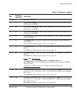
Table 4-9 Configuration register 2 (continued)
Bits
Power-on
reset state
Description