


Hardware Description
3-46 Copyright © 2003-2007 ARM Limited. All rights reserved. ARM DUI 0224F
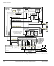
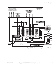
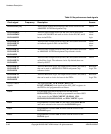
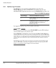
Table 3-6 Asynchronous clock signals
Clock signal Frequency Description Source
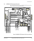
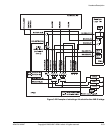
HCLKCTRL[7:0] - These signals control the multiplexor that selects clocks for the
ARM926EJ-S PXP Development Chip.
FPGA
HCLKM1M2F
HCLKM2M2F
HCLKSMF2F
- These are FPGA input clocks (for M1, M2, and S) that can be
routed to HCLKxM2F and used as clocks for the M1, M2, and S
buses in the FPGA.
Clock
select
logic
HCLKM1F2F
HCLKM2F2F
HCLKSF2F
- These are FPGA output clocks (for M1, M2, and S) that can be used
as feedback signals to DLLs in the FPGA.
Clock
select
logic
HCLKM1F2S
HCLKM2F2S
HCLKSF2S
- These are FPGA output clocks (for M1, M2, and S) that can be used
as ARM926EJ-S PXP Development Chip reference clocks.
FPGA
HCLKM1F2L
HCLKM2F2L
HCLKSF2L
- These are FPGA output clocks (for M1, M2, and S) that can be used
as RealView Logic Tile reference clocks. By default, these are
driven by OSC0.
FPGA
HCLKM1L2S
HCLKM2L2S
HCLKSL2S
- These are RealView Logic Tile output clocks (for M1, M2, and S)
that can be used as ARM926EJ-S PXP Development Chip
reference clocks.
RealView
Logic Tile
HCLKM1L2F
HCLKM2L2F
HCLKSL2F
- These are RealView Logic Tile output clocks (for M1, M2, and S)
that can be used as clocks for buses in the FPGA.
RealView
Logic Tile
ICS307 control
signals
- The signals ICS307_CLK, ICS307_DATA, and
ICS307_STRB[4:0] clock data from the SYS_OSCx registers in
the FPGA to the programmable oscillators.
OSC0 For the image provided with the FPGA and the default
HCLKCTRL[7:0] value of
0xE0
, programmable oscillator OSC0
is the source for the XTALCLKEXT, GLOBAL_CLK,
HCLKM1, HCLKM2, HCLKS, and PLLCLKEXT signals.
OSC1 Programmable oscillator OSC1 is the source for PLLCLKEXT
and can be selected as the source for the HCLKM1 signal.
OSC2 Programmable oscillator OSC2 can be used the source for the
HCLKM2 signal.
OSC3 Programmable oscillator OSC3 can be used the source for the
HCLKS signal.