


Hardware Description
3-48 Copyright © 2003-2007 ARM Limited. All rights reserved. ARM DUI 0224F
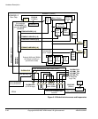
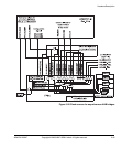
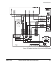
ICS307 programmable clock generators
Five programmable (6–200 MHz) clocks are supplied to the FPGA by the
programmable MicroClock ICS307 clock generators (OSC0–OSC4):
OSCCLK0 This is the default reference clock for XTALCLKDRV. This is normally
used as GLOBALCLK, the external AHB bridge clocks, and the
reference for the PLL that generates CPUCLK.
OSC0 uses a 24MHz crystal as its reference. A fixed-frequency 24MHz
signal, REFCLK24MHZ, is output from OSC0 and used as a reference
signal for:
• The input for programmable oscillators OSC1–OSC4.
• the USB controller clock
• the USB debug controller clock
• the external peripheral clocks for the SCI, UART, and SSP in the
ARM926EJ-S PXP Development Chip.
• the input to divide-by-24 logic in the FPGA that produces the
1MHz reference clock for the timers.
OSCCLK1 An alternative reference clock for the AHB M1 bridge clocks from the
FPGA to the clock selection multiplexors (HCLKM1F2S,
HCLKM1F2F, and HCLKM1F2L). By default, this clock is not used
and the AHB M1 bridge operates in synchronous mode.
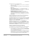
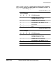
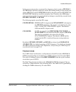
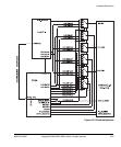
Table 3-9 HCLKS selection
HCLKCTRL signal
[4] [0] [3] [7] HCLKS driven by:
11
XX
GLOBALCLK (driven from tile,
nGLOBALCLKEN pulled HIGH)
10
XX
GLOBALCLK (driven from OSC0)
0X1X
HCLKSL2S and HCLKSL2F (from tile)
0X01
OSC0 (default)
0X00
OSC3