


Programmer’s Reference
4-54 Copyright © 2003-2007 ARM Limited. All rights reserved. ARM DUI 0224F
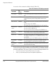
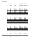
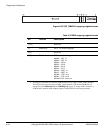
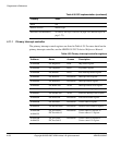
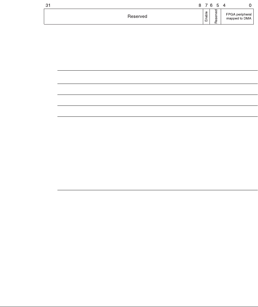
Figure 4-22 SYS_DMAP0-2 mapping register format
Table 4-34 DMA mapping register format
Bit Access Description
[31:8] - Reserved
[7] Read/write Set to 1 to enable mapping
[6:5] - Reserved
[4:0] Read/write FPGA peripheral mapped to this channel
b00000 = AACI Tx
b00001 = AACI Rx
b00010 = USB A
a
b00011 = USB B
b00100 = MCI 0
b00101 = MCI 1
b00110 = UART3 Tx
b00111 = UART3 Rx
b01000 = SCI0 int A
b01001 = SCI0 int B
b01010–b11111 Reserved
a. The OTG243 controller provides three USB interfaces, OTG (USB1), USB2, USB3, and OTG.
The OTG243, however, has only two DMA control channels, USB A and USB B, that are
managed by the USBDACK[1:0] and USBDRQ[1:0] signals. To assign a DMA channel to a
USB interface, both the DMA mapping register and the OTG243 must be programmed.