Hardware Description
ARM DUI 0224F Copyright © 2003-2007 ARM Limited. All rights reserved. 3-49
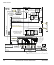
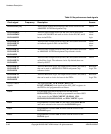
OSCCLK2 An alternative reference clock for PLLCLKEXT. This clock can be
selected as the source for CPUCLK if the ARM926EJ-S PXP
Development Chip is in low-power emulation mode.
This is also the alternative reference clock for the AHB M2 bridge clocks
from the FPGA to the clock selection multiplexors (HCLKM2F2S,
HCLKM2F2F, and HCLKM2F2L). By default, this clock is not used
and the AHB M2 bridge operates in synchronous mode.
OSCCLK3 An alternative reference clock for the AHB S bridge clocks from the
FPGA to the clock selection multiplexors (HCLKSF2S, HCLKSF2F,
and HCLKSF2L). By default, this clock is not used and the AHB S
bridge operates in synchronous mode.
OSCCLK4 This the reference for the CLCD controller (a buffered version of this
clock is output to the ARM926EJ-S PXP Development Chip as
CLCDCLKEXT).
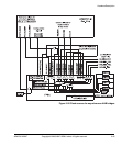
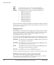
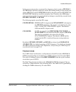
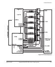
The output frequencies of the ICS307s are controlled by divider values loaded into the
serial data input pins on the oscillators. The divider values are defined by the
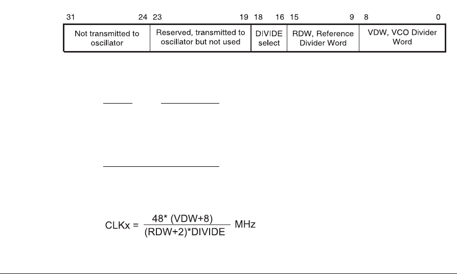
SYS_OSCx and SYS_OSCRESETx registers. The data stream and register format is
shown in Figure 3-21. See Oscillator registers, SYS_OSCx on page 4-23 for details on
the clock control registers.
Figure 3-21 Serial data and SYS_OSCx register format
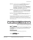
Note
Bit 23 is loaded into the shift register first and bit 0 is loaded last. Data is clocked into
the ICS307DATA pins of the oscillators on the rising edge of ICS307CLK. One of the
ICS307STRB[4:0] signals is pulsed HIGH to latch the serial data into the divider
control register.
You can calculate the oscillator output frequency from the formula:


