


Programmer’s Reference
4-92 Copyright © 2003-2007 ARM Limited. All rights reserved. ARM DUI 0224F
4.22.1 Register values
Table 4-66 to Table 4-70 on page 4-93 lists the register values for the SSMC for typical
operation of static memory devices and with a 35MHz system clock.
Note
The platform.a library contains memory setup routines. See Building an application
with the platform library on page 2-25.
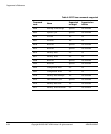
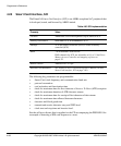
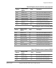
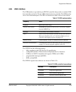
Table 4-66 Register values for Disk-on-Chip
Address
Name of SSMC
register
Value Description
+0x00 SMBIDCYR0
0x0
Idle Cycle Control Register for bank 0
+0x04 SMBWSTRDR0
0x4
Read Wait State Control Reg bank 0
+0x08 SMBWSTWRR0
0x2
Write Wait State Control Reg Bank 0
+0x0c SMBWSTOENR0
0x1
Output Enable Assertion Delay 0
+0x10 SMBWSTWENR0
0x1
Write Enable Assertion Delay 0
+0x14 SMBCR0
0x303011
Control Register for memory bank 0
+0x1c SMBWSTBRDR0
0x0
Burst Read Wait state Control Reg 0
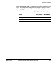
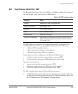
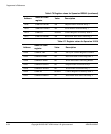
Table 4-67 Register values for Intel flash, standard async read mode, no bursts
Address
Name of SSMC
register
Value Description
+0xE0 SMBIDCYR7
0x0
Idle Cycle Control Register for bank 1
+0xE4 SMBWSTRDR7
0x4
Read Wait State Control Reg bank 1
+0xE8 SMBWSTWRR7
0x3
Write Wait State Control Reg Bank 1
+0xEc SMBWSTOENR7
0x0
Output Enable Assertion Delay 1
+0xF0 SMBWSTWENR7
0x1
Write Enable Assertion Delay 1
+0xF4 SMBCR7
0x303021
Control Register for memory bank 1
+0xFC SMBWSTBRDR7
0x0
Burst Read Wait state Control Reg 1