Hardware Description
ARM DUI 0224F Copyright © 2003-2007 ARM Limited. All rights reserved. 3-81
3.17 Smart Card interface, SCI
The ARM926EJ-S PXP Development Chip contains a PrimeCell Smart Card Interface
(SCI). A second SCI is implemented in the FPGA.
There are two sets of Smart Card connectors on the board, J25/J48 and J26/J49. Only
one header is fitted for each channel. The connector numbers refer to different size
connectors that can be can be fitted. (J25 and J26 are large connectors. J48 and J49 are
small connectors.)
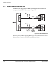
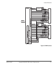
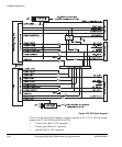
Figure 3-35 on page 3-82 shows the tristate buffers that are used to provide the interface
between the SCI and the cards. The 16-way box header J28 enables you to monitor the
signals or to connect an off-board smart card connector.
SCI0 output signals go to both the RealView Logic Tile connectors and the Smart Card
connector. The signals from the SC0 connector to the interface can be disabled by a tile
pulling nDRVEN1 HIGH. This enables a RealView Logic Tile to implement a device
that communicates with the ARM926EJ-S PXP Development Chip using the Smart
Card interface protocol.


