


Hardware Description
3-80 Copyright © 2003-2007 ARM Limited. All rights reserved. ARM DUI 0224F
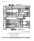
3.16 Serial bus interface
The FPGA implements a serial bus interface that is used to identify the memory
expansion modules and read and set the time-of-year clock.
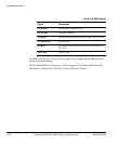
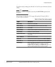
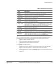
Each device on the serial bus has its own slave address. The unique address for each
slave on the serial bus is shown in Table 3-19.
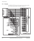
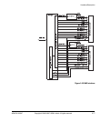
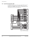
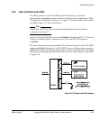
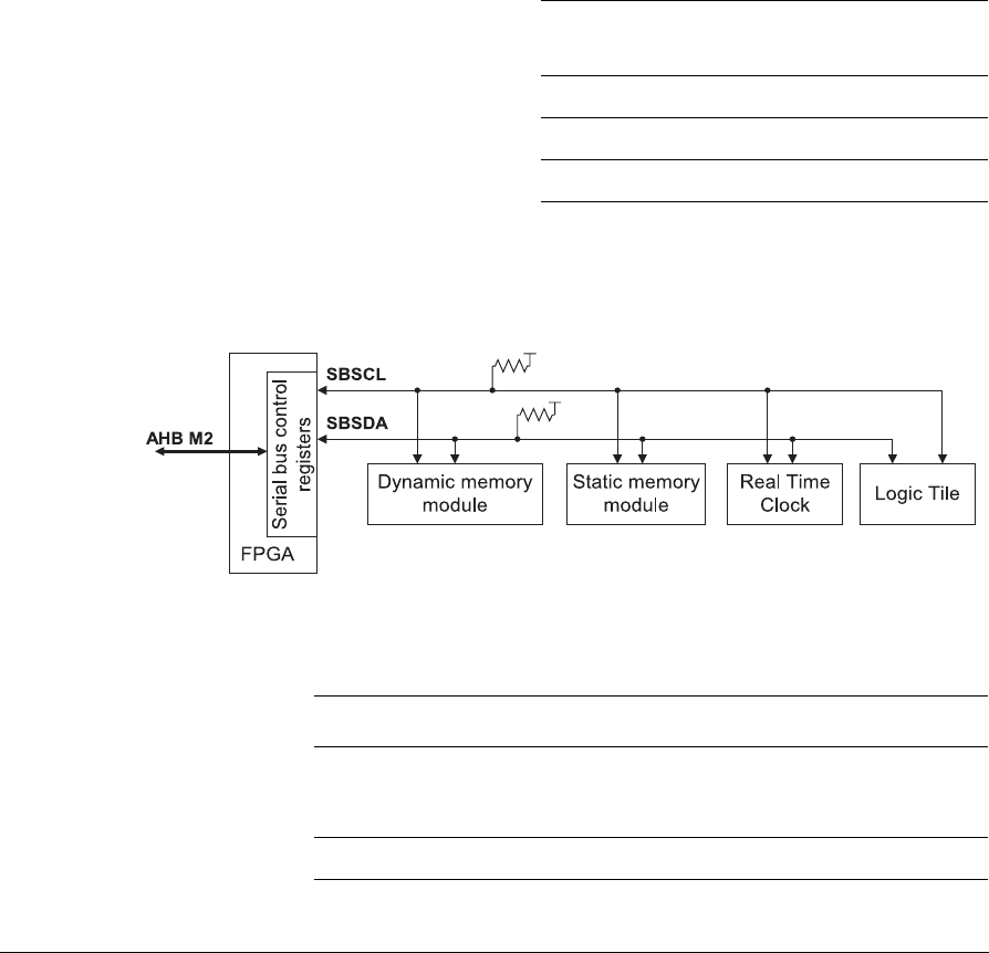
The block diagram of the interface is shown in Figure 3-34. See Serial bus interface on
page 4-86 for more information on the programming interface. The two serial bus
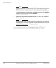
signals are described in Table 3-20.
Figure 3-34 Serial bus block diagram
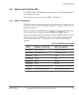
Table 3-19 Serial bus addresses
Slave address
(7-bit)
Slave device
b1010000
Dynamic memory module
b1010001
Static memory module
b1101000
Time-of-year clock
Table 3-20 Serial bus signals
Signal Description
SBSCL Open-collector clock. This clock is driven by the FPGA, but can be
held LOW by an external device if it is not ready to receive or
transmit data
SBSDA Open-collector data signal.