


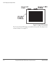
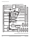
CLCD Display and Adaptor Board
C-8 Copyright © 2003-2007 ARM Limited. All rights reserved. ARM DUI 0224F
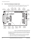
SWITCHED_VDD_NEG
This –5V to –28V supply is generated from 5V. It can be enabled by
VDDNEGSWITCH in SYS_CLCD or permanently enabled by link 14.
SWITCHED_VDD_POS
This 11V to 28V supply is generated from 5V. It can be controlled by the
touchscreen D/A converter or manually with a pot. It can be enabled by
VDDPOSSWITCH in SYS_CLCD or permanently enabled by link 11.
This supply is used to generate the STN bias voltage.
LCD_IO_VDD and Buffer I/O voltage
This is the voltage to the interface logic on the adaptor board and the
display. Link 16 selects the adaptor board interface level as CLPWR or
FIXED. Link 3 selects the display interface level as
SWITCHED_FIXED or SWITCHED_CLPWR.
Caution
Link 3 and link 16 must be set to use the same power source.
INV_IO This is the voltage to the interface logic on the prototype board. Link 2
selects the level as 5V or 3.3V.
Note
The I/O signals to the CLCD adaptor board pass through tri-state buffers. The buffers
must be powered from the same IO voltage as that required by the CLCD. This enables
the translation of the IO signals from the 3V3 signal levels present on the PB926EJ-S.
The buffers are enabled by LCDIOON in SYS_CLCD.
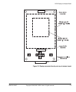
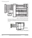
Figure C-6 on page C-10 shows the block diagram of the adaptor board power-control
circuitry.