


Hardware Description
ARM DUI 0224F Copyright © 2003-2007 ARM Limited. All rights reserved. 3-97
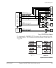
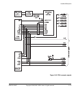
• the JTAG signals are routed through the ARM926EJ-S PXP Development Chip
• a debugger, RealView Debugger for example, controls the scan chain
• The PLDs and FPGAs are not visible on the scan chain unless they contain
debuggable devices
• If RealView Logic Tiles are present and have debuggable devices, the D_x signals
are part of their JTAG scan chain
• the FPGAs in the system load their images from configuration flash.
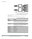
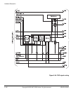
JTAG configuration mode
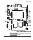
This mode is selected if the CONFIG link is fitted (see Figure 3-42 on page 3-95).
Note
The CONFIG link has been replaced by a switch on some board versions. The switch
must be in the ON position to select JTAG configuration mode.
In configuration mode:
• The signal nCFGEN is low.
• The CONFIG LED is lit on the PB926EJ-S (and on each tile in the stack).
• The JTAG scan path is rerouted to include configurable devices.
• A configuration utility, ProgCards for example, controls the scan chain.
• If RealView Logic Tiles are present, the C_x signals are part of the JTAG scan
chain.
• All FPGAs and PLDs in the system (including any devices in a RealView Logic
Tile) are added into the scan chain.
• The TAP controller in the ARM926EJ-S PXP Development Chip is not visible
and is replaced by a Boundary Scan TAP controller that is used for board-level
production testing.
• This enables the board to be configured or upgraded in the field using JTAG
equipment or the onboard USB debug port.
• The nonvolatile PLDs devices can be reprogrammed directly by JTAG.
• FPGA images can be loaded from the scan chain.