


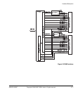
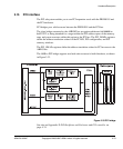
Hardware Description
ARM DUI 0224F Copyright © 2003-2007 ARM Limited. All rights reserved. 3-83
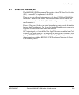
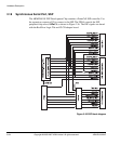
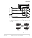
The default setting is linking pins AB. Both 3.3V and 5V cards will function with this
setting.
Note
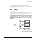
The Smart Card VCC is switched on and off by the SCIVCCENx signal from the
PrimeCell.
See also Smart Card Interface, SCI on page 4-88 and the SCI PrimeCell PL131
Technical Reference Manual.
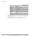
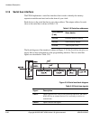
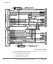
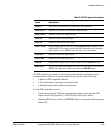
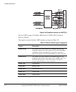
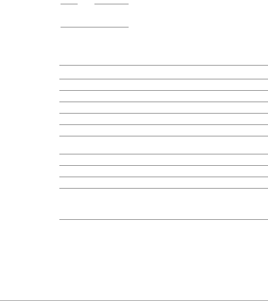
Table 3-21 Smart Card interface signals
Signal Description
SCICLKINx PrimeCell SCI clock input.
nSCICLKENx Tristate output buffer control for clock (active LOW).
SCICLKOUTx Clock output.
nSCIDATAENx Tristate control for external off-chip buffer (active LOW).
SCIDATAINx PrimeCell SCI serial data input.
nSCIDATAOUTENx Data output enable (typically drives an open-drain configuration,
active LOW).
nSCICARDRSTx Reset to card (active LOW).
SCIFCBx Function code bit, used in conjunction with nSCICARDRST.
SCIDETECTx Card detect signal from card interface device (active HIGH).
nDRVINEN0 Device select signal from RealView Logic Tile. This signal can
be driven HIGH by the logic tile to enable it to drive the
SCIDATAIN0, SCICLKIN0, and SCIDETECT0 signals. The
signal is normally pulled LOW by a resistor to ground.