


Introduction
1-8 Copyright © 2003-2007 ARM Limited. All rights reserved. ARM DUI 0224F
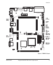
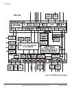
1.2.6 Memory
The volatile memory system includes SSRAM and SDRAM memory. You can expand
this memory by installing external static or dynamic memory expansion boards.
The nonvolatile memory system consists of 64MB of 32-bit flash and 64MB of 16-bit
NAND Disk-on-Chip flash. The flash is managed by the static memory controller in the
ARM926EJ-S PXP Development Chip. You can expand the flash memory by installing
an external static memory expansion board. See Appendix E Memory Expansion
Boards.
1.2.7 Clock generators
The PB926EJ-S contains the following clock sources:
• crystal oscillators (these are the reference frequencies for the Real Time Clock,
USB, AACI, Ethernet, and programmable oscillators)
• five programmable ICS307 clock sources. Two of these are used as the reference
for the CPU system clock in the ARM926EJ-S PXP Development Chip and the
CLCD controller clock. The other three programmable clocks can be used as
external reference clocks for the AHB buses.
• if fitted, the PCI backplane or RealView Logic Tiles. The external clocks can be
selected as the reference clocks for the PB926EJ-S.
See Clock architecture on page 3-35.
1.2.8 Debug and test interfaces
The JTAG connector enables JTAG hardware debugging equipment, such as Multi-ICE
or RealView ICE, to be connected to the PB926EJ-S. The JTAG signals can also be
controlled by the on-board USB debug port controller. See JTAG and USB debug port
support on page 3-96.
A Mictor connector on the PB926EJ-S enables monitoring of the ARM926EJ-S PXP
Development Chip Embedded Trace Macrocell (ETM9) signals by a Trace Port
Analyzer (TPA). The trace port is medium trace size (16-bit packet). See Trace
connector pinout on page A-37 for connection information.