


Specifications
ARM DUI 0224F Copyright © 2003-2007 ARM Limited. All rights reserved. B-7
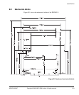
B.2.2 Memory timing
Table B-6 shows the memory timing. For more detail on timing and example
waveforms, see the ARM PrimeCell Static Memory Controller (PL093) Technical
Reference Manual and the ARM PrimeCell Multiport Memory Controller (GX175)
Technical Reference Manual.)
B.2.3 Peripheral timing
Table B-7 on page B-8 shows the peripheral and controller timing. For more detail on
timing and example waveforms, see the relevant Technical Reference Manual for the
module.
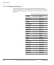
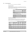
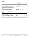
Table B-6 ARM926EJ-S PXP Development Chip memory timing
Memory signals Clock tov toh tis tih
SSMC outputs (SMDATA[31:0] for write,
nSMDATAEN[3:0], SMADDR[25:0], SMCS[7:0],
nSMOEN, nSMWEN, nSMBLS[3:0], and
CANCELSMWAIT)
SMCLK is typically 70MHz for a
t
cyc
of 14.3ns.
SMCLK 10ns 1ns - -
SSMC inputs in asynchronous mode (SMDATA[31:0] for
read, SMWAIT, and CANCELSMWAIT)
SMCLK - - 5ns 1ns
SSMC inputs in synchronous mode (SMDATA[31:0] for read,
SMWAIT, and CANCELSMWAIT)
Note
The SMFBCLK delay from SMCLK must be less than 1.5ns.
SMFBCLK - - 5ns 1ns
MPMC outputs (MPMCADDROUT[27:0],
MPMCCKEOUT[3:0], MPMCDQMOUT[3:0],
nMPMCOEOUT, nMPMCRASOUT, nMPMCRPOUT,
nMPMCWEOUT, MPMCDATA[31:0] for write )
MPMCCLK is typically 70MHz for a
t
cyc
of 14.3ns.
MPMCCLK 4ns 0.5ns - -
MPMC inputs (MPMCFBCLKIN[3:0],
MPMCTESTREQA, for read)
Note
The MPMCFBCLK delay from MPMCCLK must be less
than 1.5ns.
MPMCFBCLK - - 1ns 0.5ns