Hardware Description
3-18 Copyright © 2003-2007 ARM Limited. All rights reserved. ARM DUI 0224F
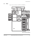
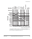
For details on FPGA components, see:
• FPGA configuration
• Reset controller on page 3-22
• Clock architecture on page 3-35
• Advanced Audio Codec Interface, AACI on page 3-56
• Character LCD controller on page 3-59
• Ethernet interface on page 3-68
• Keyboard/Mouse Interface, KMI on page 3-74
• Memory Card Interface, MCI on page 3-75
• PCI interface on page 3-79
• Smart Card interface, SCI on page 3-81
• User switches and LEDs on page 3-87
• UART interface on page 3-88
• USB interface on page 3-92.
Note
The ARM926EJ-S PXP Development Chip and FPGA buses on the PB926EJ-S are
shared with the Logic Tile headers. If you are using a Logic Tile, ensure that the tile
manages the bus signals correctly (AHB buses used by the FPGA and RealView Logic
Tiles on page F-11).
3.2.1 FPGA configuration
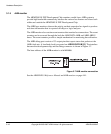
At power-up the FPGA loads its configuration data from a flash memory device.
Parallel data from the flash memory is streamed by the configuration PLD into the
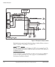
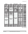
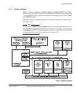
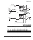
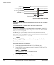
configuration ports of the FPGA. Figure 3-9 on page 3-19 and Figure 3-10 on page 3-20
show the FPGA configuration mechanism. The image loaded into the FPGA is
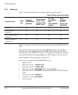
determined by configuration switches S1-6 and S1-7 as listed in Table 3-2 on page 3-19.


