


Signal Descriptions
A-34 Copyright © 2003-2007 ARM Limited. All rights reserved. ARM DUI 0224F
This section contains the following subsections:
• Overview of test points
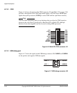
• JTAG on page A-36
• USB debug port on page A-36
• Trace connector pinout on page A-37
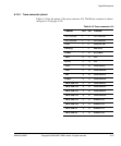
• Embedded logic analyzer on page A-38
• AHB monitor on page A-38
• FPGA debug connector pinout on page A-40.
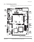
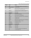
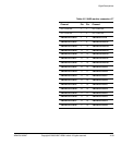
A.13.1 Overview of test points
The functions of the test points on the PB926EJ-S are summarized in Table A-13. For
information about setting the frequency of the core clock and auxiliary clock see Clock
architecture on page 3-35.
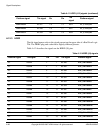
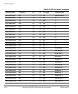
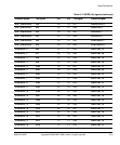
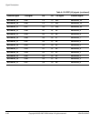
Table A-13 Test point functions
Test point Signal Function
TP1 VBATT 1.5V backup battery voltage for RTC
TP2 REFCLK32K Output from the 32kHz oscillator module
TP3 XTALCLK Buffered GLOBALCLK
TP4 OSCCLK0 Output from programmable oscillator 0
TP5 OSCCLK1 Output from programmable oscillator 4
TP6 GLOBALCLK Global clock (the default source is XTALCLKDRV from the FPGA)
TP7 OSCCLK2 Output from programmable oscillator 2
TP8 OSCCLK3 Output from programmable oscillator 3
TP9 OSCCLK4 Output from programmable oscillator 4
TP10 REFCLK24MHZ 24MHz ICS307 reference
TP11 DXN XC2V2000 test signal (for manufacturing use only)
TP12 DXP XC2V2000 test signal (for manufacturing use only)
TP13 5V 5V power supply for ARM926EJ-S PXP Development Chip
emulation
TP14 GND Ground. OV signal