Intel
®
IXP42X product line and IXC1100 control plane processors—PCI Controller
Intel
®
IXP42X Product Line of Network Processors and IXC1100 Control Plane Processor
DM September 2006
230 Order Number: 252480-006US
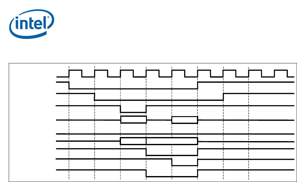
6.6.7 Initiated Memory Write Transaction
The following transaction is a PCI Memory Write Cycle initiated from the IXP42X
product line and IXC1100 control plane processors. This diagram is to understand the
inner workings of PCI transfers and may not reflect actual operation of the PCI
Controller implemented on the IXP42X product line and IXC1100 control plane
processors. The transaction is initiated to address location hexadecimal 0x00000014.
The value of binary 00 in PCI_AD (1:0) indicates that this is a linear-increment transfer
type. A hexadecimal value of 0x7 — written on the PCI_C/BE_N bus during the address
phase — signifies that this is a PCI Bus Memory Read Cycle. All byte enables are
asserted for the transaction.
Notice that on this transaction the PCI_DEVSEL_N signal timing is different. This signal-
timing differential is due to the fact that the DEVSEL_N signal must become active
within the first three clocks after the FRAME_N becoming active. This requirement
could be different for every device that is on the PCI Bus. There is also no relationship
to when TRDY_N becomes active other than the TRDY_N signal must not become active
prior to the DEVSEL_N signal becoming active.
Figure 39. Initiated PCI Memory Read Cycle
PCI_CLK
PCI_FRAME_N
PCI_AD (31:0)
PCI_IDSEL
PCI_C/BE_N
PCI_IRDY_N
PCI_TRDY_N
PCI_DEVSEL_N
0x00000014
DAT
A
0x6 0x0
PCI_REQ_N
PCI_GNT_N


