Intel
®
IXP42X Product Line of Network Processors and IXC1100 Control Plane Processor
September 2006 DM
Order Number: 252480-006US 287
SDRAM Controller—Intel
®
IXP42X product line and IXC1100 control plane processors
7.4 Register Description
The IXP42X product line and IXC1100 control plane processors’ SDRAM interface is
programmed through a set of configuration registers that are described in the following
sections. Many timing parameters are encoded as a number of SDM_CKE clock cycles.
The registers of the SDRAM controllers are 32-bit each. Each register access is 32-bits
only (no byte or half-word access). Therefore if software running on the Intel XScale
processor wishes to change one bit, it must read the entire contents of the register and
write them back with that one bit changed. These registers are accessible via the South
AHB interface. The table below shows the overview of the SDRAM controllers’
addresses.
7.4.1 Configuration Register
The configuration register (SDR_CONFIG) is a read/write register that contains control
bits for configuring the SDRAM. The two physical SDRAM banks must be implemented
with the same type of SDRAM devices.
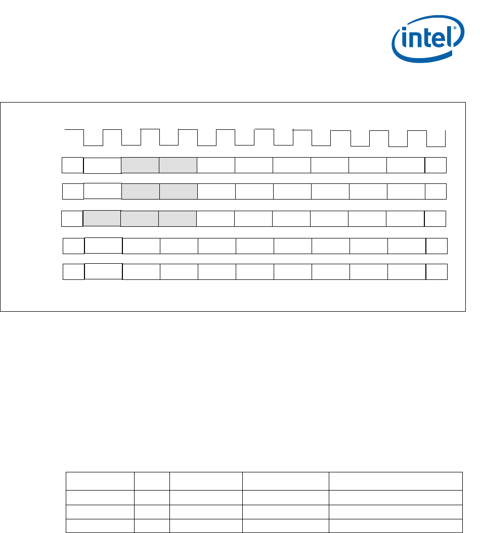
Figure 57. SDRAM Write Example
ACTIVE
NOP
NOP
WRITE WRITE WRITE WRITE WRITE WRITE
RAS
XX
XX
CAS CAS CAS CAS CAS CAS
XX
XX
XX
D0 D1
D2 D3 D4
D5
HI
HI
HI
LOW LOW
LOW LOW LOW
LOW
HI
HI
HI
HI HI
HI HI HI
HI
SDM_CLK
COMMAND
SDM_ADDR
SDM_DATA
SDM_DQM
SDM_CKE
Table 113. SDRAM Register Overview
Register Name R/W Reset Hex Value Hex Address Description
sdr_config R/W 0x00000010 0xCC000000 SDRAM Configuration Register
sdr_refresh R/W 0x00000384 0xCC000004 SDRAM Refresh Register
sdr_ir R/W 0x00000000 0xCC000008 SDRAM Instruction Register


